Organic electroluminescence type display apparatus

A display device and luminescent technology, applied in the direction of electroluminescent light source, electric light source, measuring device, etc., can solve the problems of high light reflectivity, unobtainable, difficult metal, etc., achieve high reflection efficiency and improve injection efficiency

Inactive Publication Date: 2006-08-30
MITSUBISHI ELECTRIC CORP
View PDF6 Cites 12 Cited by
  • Summary
  • Abstract
  • Description
  • Claims
  • Application Information

AI Technical Summary

Problems solved by technology

In order to solve this problem, when the method of adding another metal film between the conductive oxide film and the Al alloy film is adopted, since it is difficult to optimize the light reflectance of the metal, there is a problem that the necessary high light reflectance cannot be obtained on the anode.

Method used


Image

  • Organic electroluminescence type display apparatus
  • Organic electroluminescence type display apparatus
  • Organic electroluminescence type display apparatus

Examples


Embodiment 1

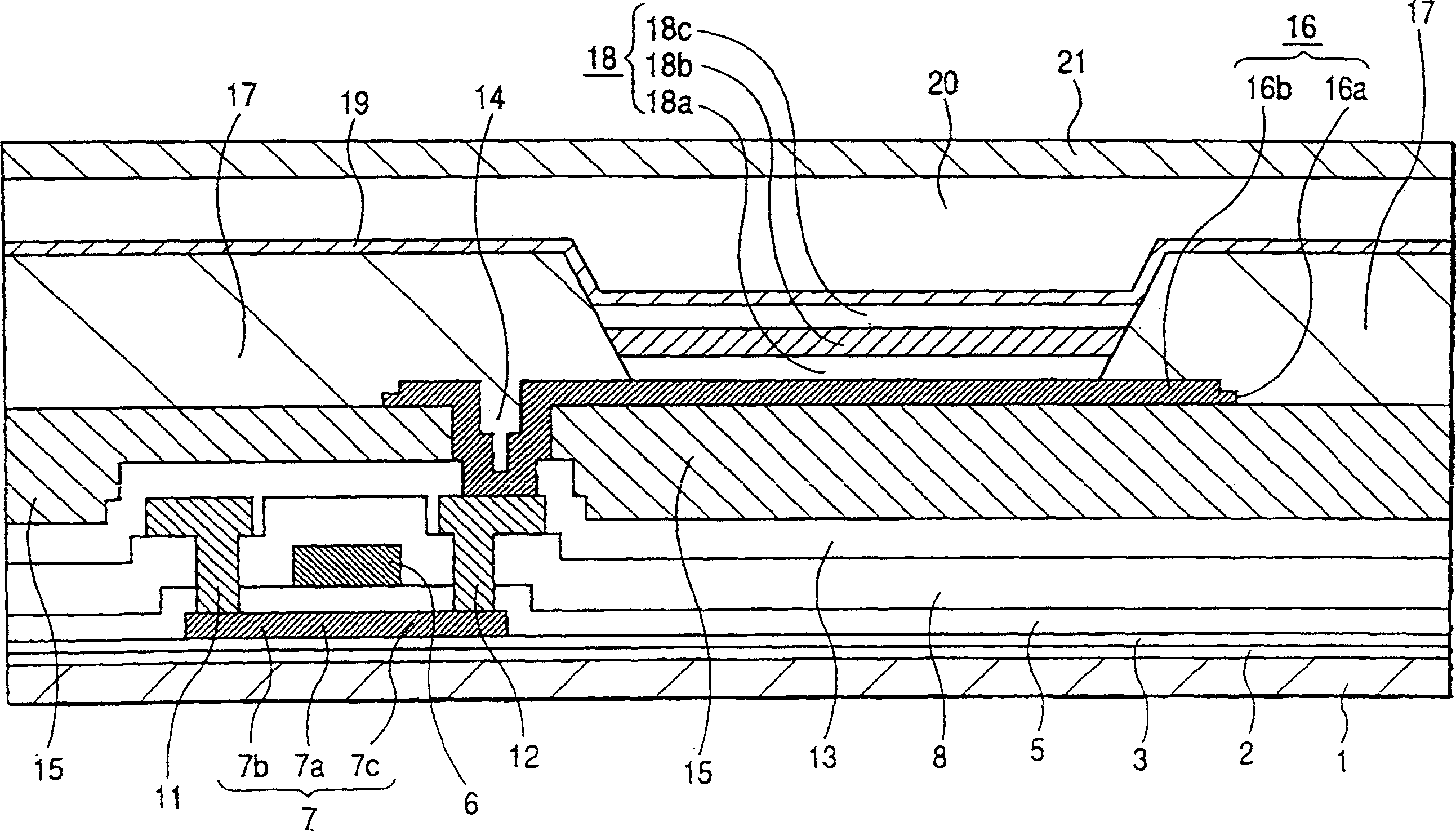
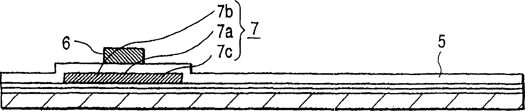
[0032] figure 1 It is a cross-sectional view showing a TFT substrate constituting the organic electroluminescent display device according to Example 1 of the present invention and a pixel portion of an organic EL element formed on top of the TFT substrate. figure 1 Among them, the transparent insulating film formed on the insulating substrate 1, that is, the SiN film 2, SiO 2 On the film 3, a polysilicon film 7 including a channel region 7a, a source region 7b, and a drain region 7c is provided. covered SiO 2 film 3 or polysilicon film 7 to form a gate insulating film 5, and a gate electrode 6 is formed on its top layer, made of SiO 2 The first interlayer insulating film 8 composed of etc. The source electrode 11 and the drain electrode 12 are on the first interlayer insulating film 8 and are respectively connected to the source region 7b and the drain region 7c through the contact holes 9 and 10, forming a thin film transistor based on the above structure. Also, the top l...


PUM

PropertyMeasurementUnit
thicknessaaaaaaaaaa
thicknessaaaaaaaaaa
mean roughnessaaaaaaaaaa

Abstract

An organic electroluminescence type display apparatus of top emission type, in which a thin film transistor (TFT), a flattening film (15) made of organic resin and an organic EL element, in which at least an anode (16), an electroluminescence layer (18) and a cathode (19) are laminated on the flattening film in this order, are formed in each picture element in a display region on a substrate. The anode is composed of at least two layer film including an aluminium alloy film (16a) containing as a impurity at least one of transition metals of the eighth group of 3d into Al and including a light transmitting conductive oxide film (16b) laminated on the Al alloy film.

Description

technical field [0001] The present invention relates to an electro-optic display device, and in particular to an organic electroluminescence (EL) element (hereinafter referred to as an organic EL element) formed as an electro-optic element in a pixel region on an active matrix substrate on which TFTs are formed. Luminescent display device. Background technique [0002] In recent years, an organic electroluminescent display device using a luminous body such as an organic EL element as an electro-optic element is generally used as one of display screens. [0003] The basic structure of an organic EL element adopts a structure in which an electroluminescent layer including an organic EL layer is sandwiched between an anode electrode (also called an anode) and a cathode electrode (also called a cathode). By applying a voltage between the anode and the cathode, the The organic EL layer emits light by injecting holes from the anode side and injecting electrons from the cathode si...

Claims


Application Information

Patent Timeline
Patent Type & Authority Applications(China)
IPC IPC(8): H01L27/32H05B33/28
CPCH01L27/3244H01L2251/5315H01L51/5218H01L51/5271H10K59/12H10K50/818H10K50/856H10K2102/3026G08G1/0962H04M1/6075G01S19/13G08G1/0969H04M2250/52H04M2201/50H04M1/724
Inventor 长山显祐石贺展昭井上和式竹口彻渕上宏幸
Owner MITSUBISHI ELECTRIC CORP
Why Eureka
Try Eureka