Surface acoustic wave apparatus and communications equipment
a surface acoustic wave and apparatus technology, applied in the field of surface acoustic wave, can solve the problems of insufficient high power durability of the idt electrode, large amount of heat generated in the idt electrode, and accelerate the migration of the electrode material, so as to achieve efficient discharge of heat to the circuit board, excellent high power durability, and improved efficiency of the saw device.
- Summary
- Abstract
- Description
- Claims
- Application Information
AI Technical Summary
Benefits of technology
Problems solved by technology
Method used
Image
Examples
example 1
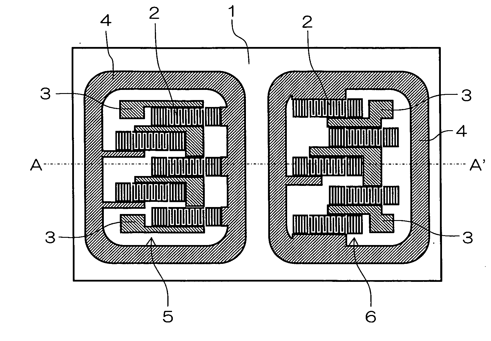
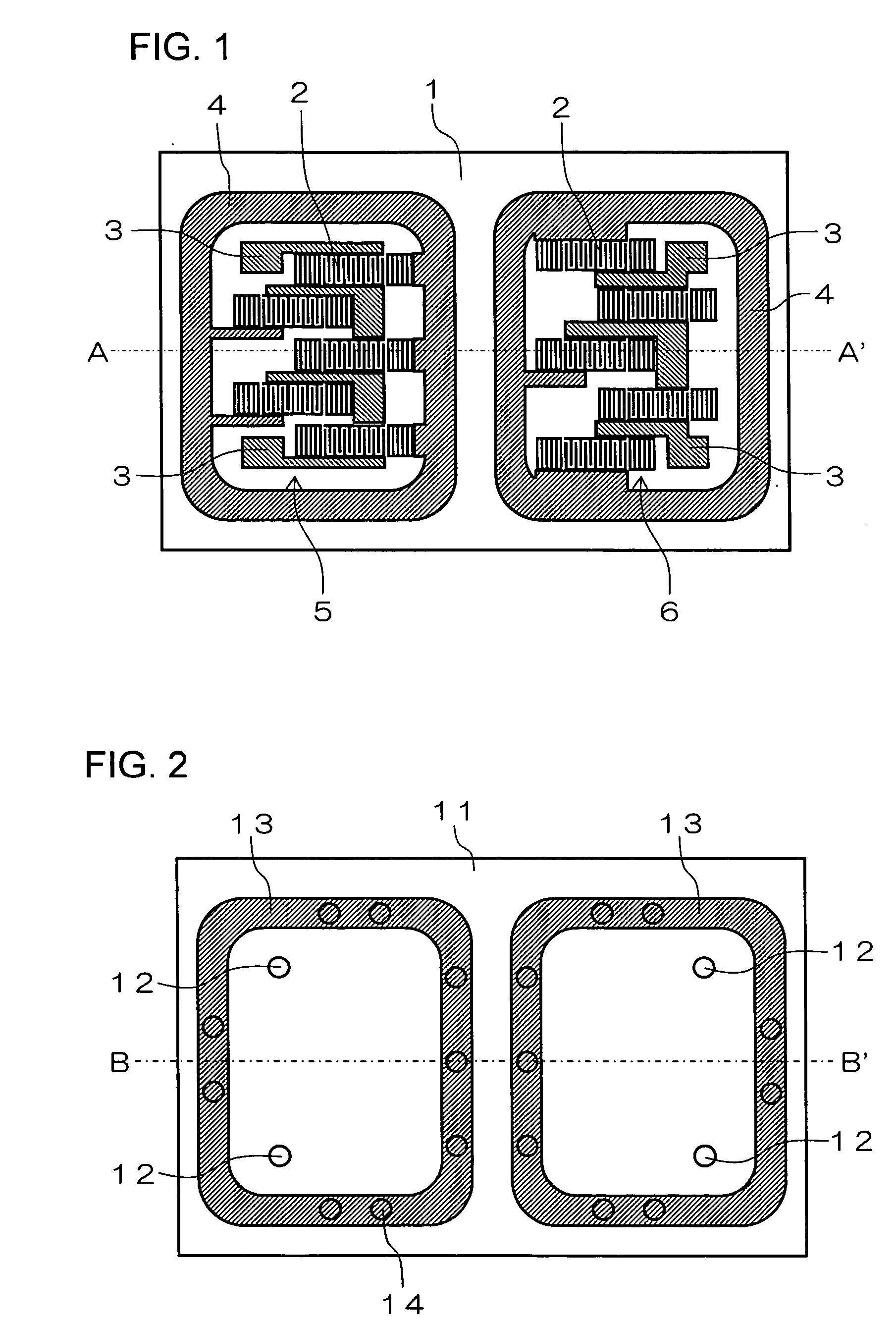
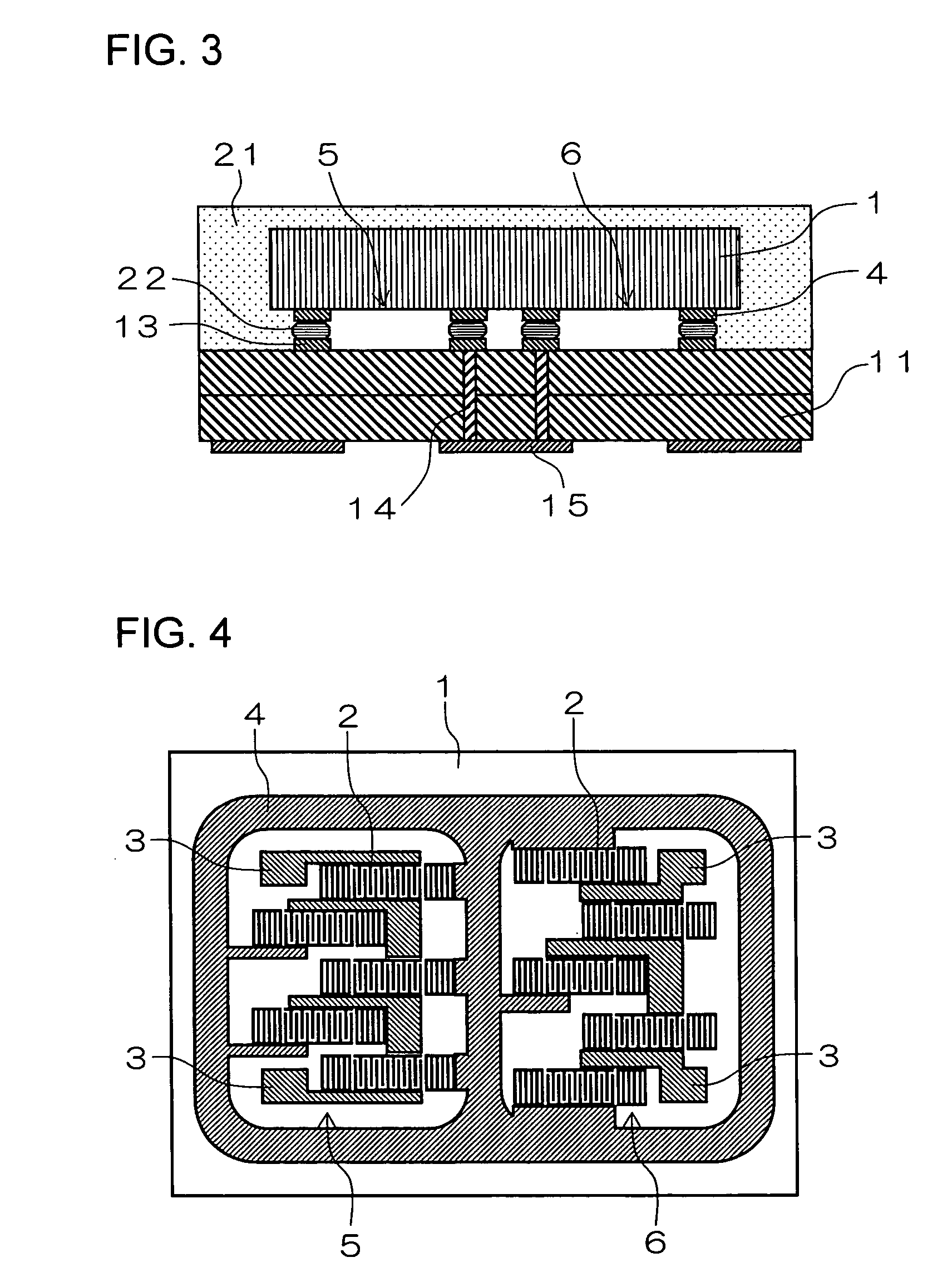
[0105] A 38.7° Y-cut X-propagating lithium tantalate single crystal substrate was used as the piezoelectric substrate. A pattern of the IDT electrodes 2, a pattern of the electrode pads as the input / output electrodes, a pattern of wiring for electrically connecting the electrodes and electrode pads, and the circular electrode, which were formed of Al alloy of Al (99 percent by mass)—Cu (1 percent by mass), were formed on the principal face of the piezoelectric substrate. After preparing these patterns an Al alloy thin film was formed according to the sputtering method as described below, photolithography was performed using a stepper, spin coater, developing apparatus and so on, and then etching was performed using an RIE (Reactive Ion Etching) apparatus to obtain each desired pattern.
[0106] First, a lithium tantalate wafer as the piezoelectric substrate was subject to ultrasonic cleaning by use of an organic solvent such as IPA (isopropyl alcohol) to clean organic constituents. Su...
example 2
[0117] Next, another example of the present invention will be described with reference to FIG. 10.
[0118] A 36° Y-cut X-propagating lithium tantalate single crystal substrate was used as the piezoelectric substrate 1. The chip size was set as 1.1 mm×1.5 mm. The IDT electrodes 2 formed of Al—Cu alloy, the input / output pad electrodes 3, the ground pad electrodes 3a, the reflectors 9, the wiring electrodes 10, the connection lines 16, and the circular electrode 4 were formed on the piezoelectric substrate 1 so as to have a thickness of 1800 Å according to the sputtering method, photolithography was performed using a stepper, spin coater, developing apparatus and so on, and then etching was performed using an RIE (Reactive Ion Etching) apparatus to obtain desired patterns.
[0119] Next, the piezoelectric substrate was diced along a dicing line and divided every chip of the SAW device.
[0120] An LTCC (Low Temperature Co-fired Ceramics) substrate having a size of 70 mm×70 mm and a thicknes...
PUM
 Abstract
Description
Claims
Application Information


