Light emitting device and method of manufacturing the same

a technology of light-emitting devices and manufacturing methods, which is applied in the field of gallium nitride, can solve the problems of decrepit optical power, high-power operation, and thermal stability degradation of devices, and achieve the effect of effectively releasing heat generated by devices, reducing the number of photons absorbed during emission, and shortening the emitting path of photons

Active Publication Date: 2010-10-21
SEOUL VIOSYS CO LTD +1
View PDF3 Cites 49 Cited by
  • Summary
  • Abstract
  • Description
  • Claims
  • Application Information

AI Technical Summary

Benefits of technology

[0008]The present invention provides a vertical-type light emitting device and a method of manufacturing the same, which can effectively release heat produced when the device operates and improve optical efficiency characteristics.
[0009]The present invention also provides a light emitting device and a method of manufacturing the same, which can improve heat release and optical efficiency characteristics by stacking a p-type semiconductor layer, an active layer, and an n-type semiconductor layer over a conductive support layer, and allowing light generated in the active layer to emit through the n-type semiconductor layer.
[0030]In accordance with the exemplary embodiments of the present invention, a vertical-type light emitting device includes a conductive support layer in a lower portion thereof to effectively release heat generated when the device operates. This makes it possible to realize a high-power device.
[0031]Also, since photons generated in an active layer emit through an n-type semiconductor layer, an emitting path of the photons is shortened. Thus, the number of photons absorbed during the emission can be reduced. In addition, doping concentration of the n-type semiconductor layer can be increased to improve electric conductivity, thus reducing current spreading-resistance. As a result, optical power can be improved.
[0032]Also, a p-type electrode is thickly formed on a p-type semiconductor layer to reduce current density and improve the stability of a device.

Problems solved by technology

Thus, current spreading-resistance is great in a high-power operation, decreasing optical power.
Also, since heat produced in a device operation is not effectively released through the sapphire substrate, there is a limitation that thermal stability of the device is degraded, thereby making a problem in the high-power operation.
However, the flip-chip-type package used for the flip-chip-type light emitting device causes a manufacturing process to be complicated.
Moreover, optical efficiency characteristics of the flip-chip-type light emitting device are degraded because a large amount of photons are absorbed into the sapphire substrate while the light emits from the active layer to the outside through the sapphire substrate.

Method used


Image

  • Light emitting device and method of manufacturing the same
  • Light emitting device and method of manufacturing the same
  • Light emitting device and method of manufacturing the same

Examples


first embodiment

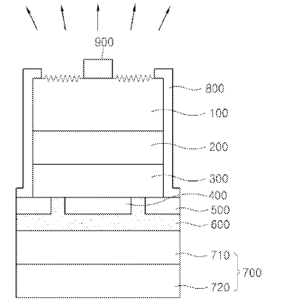
[0060]FIG. 1 is a cross-sectional view of a light emitting device in accordance with the present invention.

[0061]Referring to FIG. 1, the light emitting device in accordance with the first embodiment includes an n-type semiconductor layer 100, an active layer 200, a p-type semiconductor layer 300, a p-type electrode layer 400, an etch stop layer 500, a cover layer 600, a support layer 700, a passivation layer 800, and an n-type electrode layer 900.

[0062]The n-type semiconductor layer 100, for injecting electrons into the active layer 200, may be a GaN layer doped with n-type impurities, e.g., Si, of the concentration ranging from approximately 1×10¹⁹ / cm3 to approximately 5×10¹⁹ / cm3, but the present invention is not limited thereto. Thus, various semi-conductive materials may be used. That is, a nitride such as GaN, InN, or AlN (group III-V), or a compound having a predetermined ratio of the nitride may be used. Alternatively, the n-type semiconductor layer 100 may be formed in a mul...

second embodiment

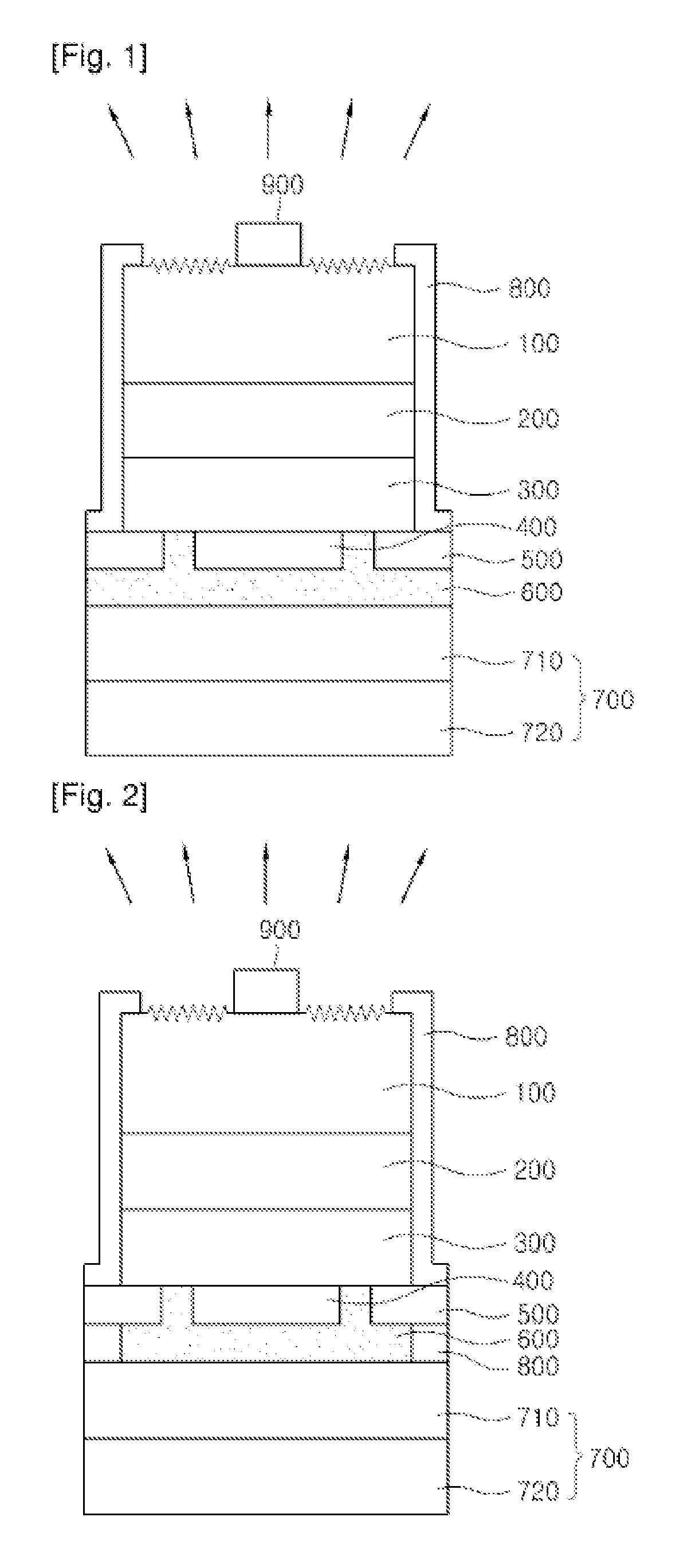
[0072]FIG. 2 is a cross-sectional view of a light emitting device in accordance with the present invention.

[0073]Referring to FIG. 2, the light emitting device in accordance with this embodiment includes an n-type semiconductor layer 100, an active layer 200, a p-type semiconductor layer 300, a p-type electrode layer 400, an etch stop layer 500, a cover layer 600, a support layer 700, a passivation layer 800, and an n-type electrode layer 900. The light emitting device in accordance with this embodiment differs from the light emitting device of FIG. 1 in that the cover layer 600 is formed to expose portions of the etch stop layer 500, and the passivation layer 800 is further formed on the portions of the etch stop layer 500 where the cover layer 600 is not formed.

third embodiment

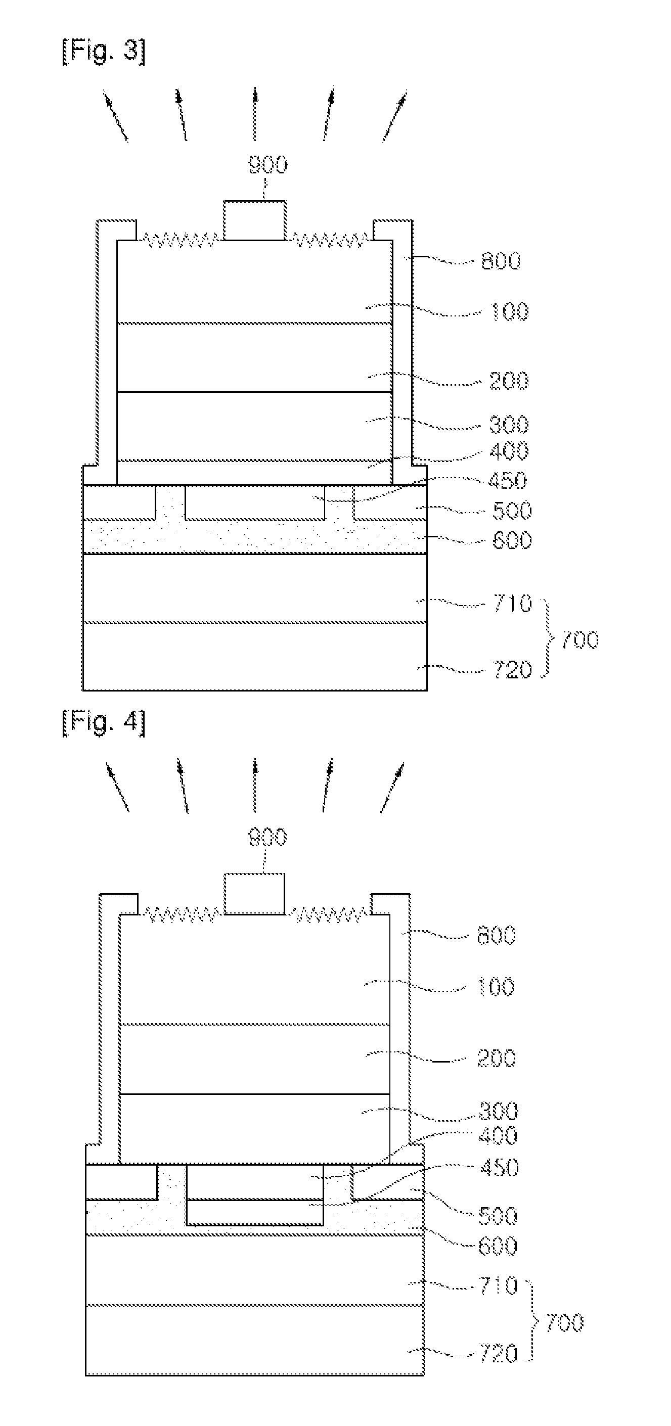
[0074]FIG. 3 is a cross-sectional view of a light emitting device in accordance with the present invention.

[0075]Referring to FIG. 3, the light emitting device in accordance with this embodiment includes an n-type semiconductor layer 100, an active layer 200, a p-type semiconductor layer 300, a p-type electrode layer 400, a reflective layer 450, an etch stop layer 500, a cover layer 600, a support layer 700, a passivation layer 800, and an n-type electrode layer 900. The light emitting device in accordance with this embodiment differs from the light emitting device of FIG. 1 in that the p-type electrode layer 400 is entirely formed on the p-type semiconductor layer 300, and the reflective layer 450 is further formed on a predetermined portion of the p-type electrode layer 400. That is, the p-type electrode layer 400 of the light emitting device of FIG. 1 includes the electrode metal and the reflective metal that are stacked, but the light emitting device in accordance with this embo...


PUM


Abstract

Provided are a vertical-type light emitting device and a method of manufacturing the same. The light emitting device includes a p-type semiconductor layer, an active layer, and an n-type semi-conductor layer that are stacked, a cover layer disposed on a p-type electrode layer to surround the p-type electrode layer, a conductive support layer disposed on the cover layer, and an n-type electrode layer disposed on the n-type semiconductor layer.

Description

CROSS-REFERENCE TO RELATED APPLICATIONS[0001]This application is the National Stage of International Application No. PCT / KR2008 / 006266, filed Oct. 23, 2008, and claims priority from and the benefit of Korean Patent Application No. 10-2007-0133138, filed on Dec. 18, 2007, and Korean Patent Application No. 10-2008-0034655, filed on Apr. 15, 2008, which are all hereby incorporated by reference for all purposes as if fully set forth herein.BACKGROUND OF THE INVENTION[0002]1. Field of the Invention[0003]The present invention relates to a light emitting device and a method of manufacturing the same, and more particularly, to a gallium nitride (hereinafter, referred to as “GaN”)-based light emitting device (LED) having a vertical-type structure and a method of manufacturing the same.[0004]2. Discussion of the Background[0005]Recently, as light emitting devices having GaN semiconductors are widely expected to replace typical light sources including incandescent lamps, fluorescent lamps, and...

Claims


Application Information

Patent Timeline
Patent Type & Authority Applications(United States)
IPC IPC(8): H01L33/02H01L33/36H01L33/42
CPCH01L33/0079H01L33/40H01L33/36H01L2933/0016H01L33/641H01L33/0093
Inventor LEE, JONG-LAM
Owner SEOUL VIOSYS CO LTD
Why Eureka
Try Eureka