Light-emitting diode device and method of manufacturing thereof

A technology of light-emitting diodes and devices, which is applied in chemical instruments and methods, luminescent materials, electric solid devices, etc., can solve the problems of reduced light extraction efficiency of LED devices, and achieve the effects of low product cost and simplified production lines

Inactive Publication Date: 2006-09-06
SHARP KK
View PDF4 Cites 9 Cited by
  • Summary
  • Abstract
  • Description
  • Claims
  • Application Information

AI Technical Summary

Problems solved by technology

However, as in the case of using the above-mentioned light-scattering agent, since the anti-sedimentation agent also contains ultrafine granular silica (SiO 2 ), light absorption will occur and lead to a decrease in the light extraction efficiency of the LED device

Method used


Image

  • Light-emitting diode device and method of manufacturing thereof
  • Light-emitting diode device and method of manufacturing thereof
  • Light-emitting diode device and method of manufacturing thereof

Examples


Embodiment Construction
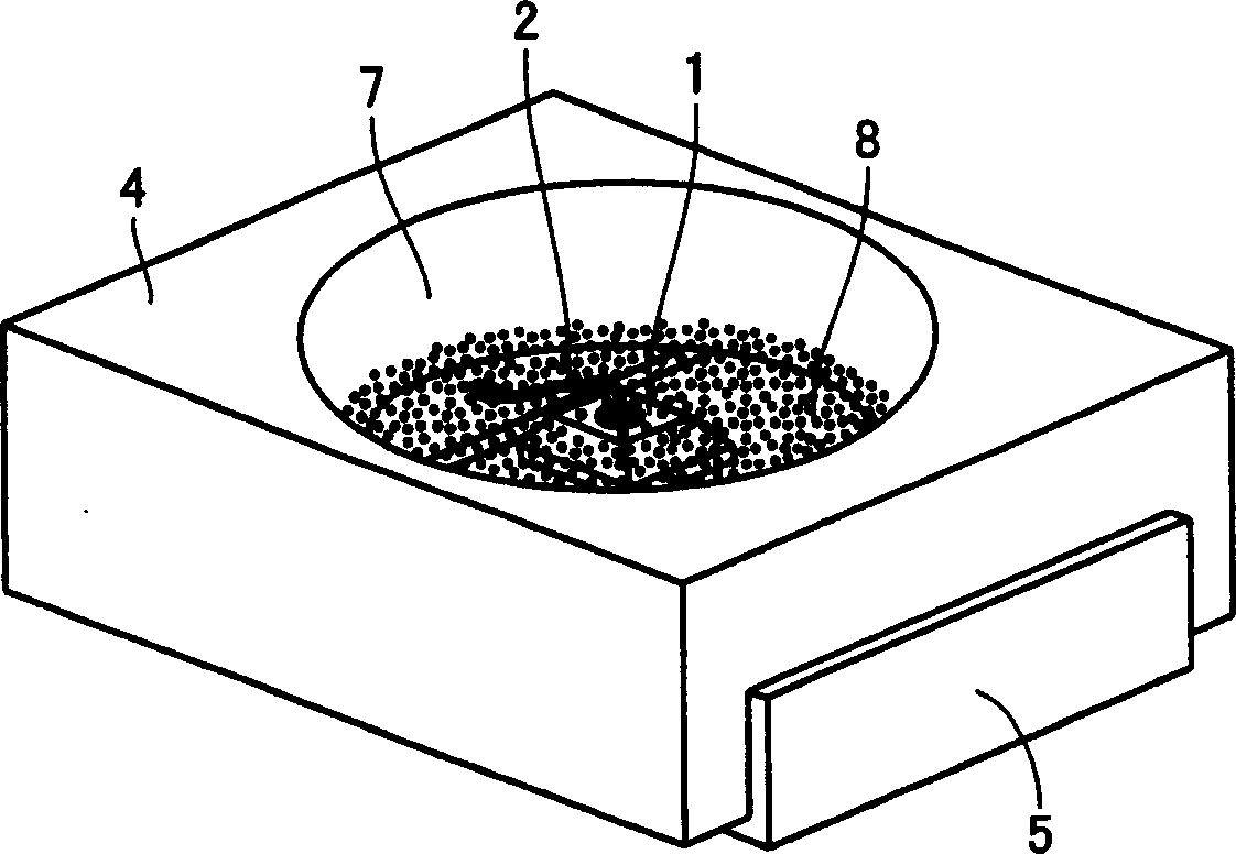
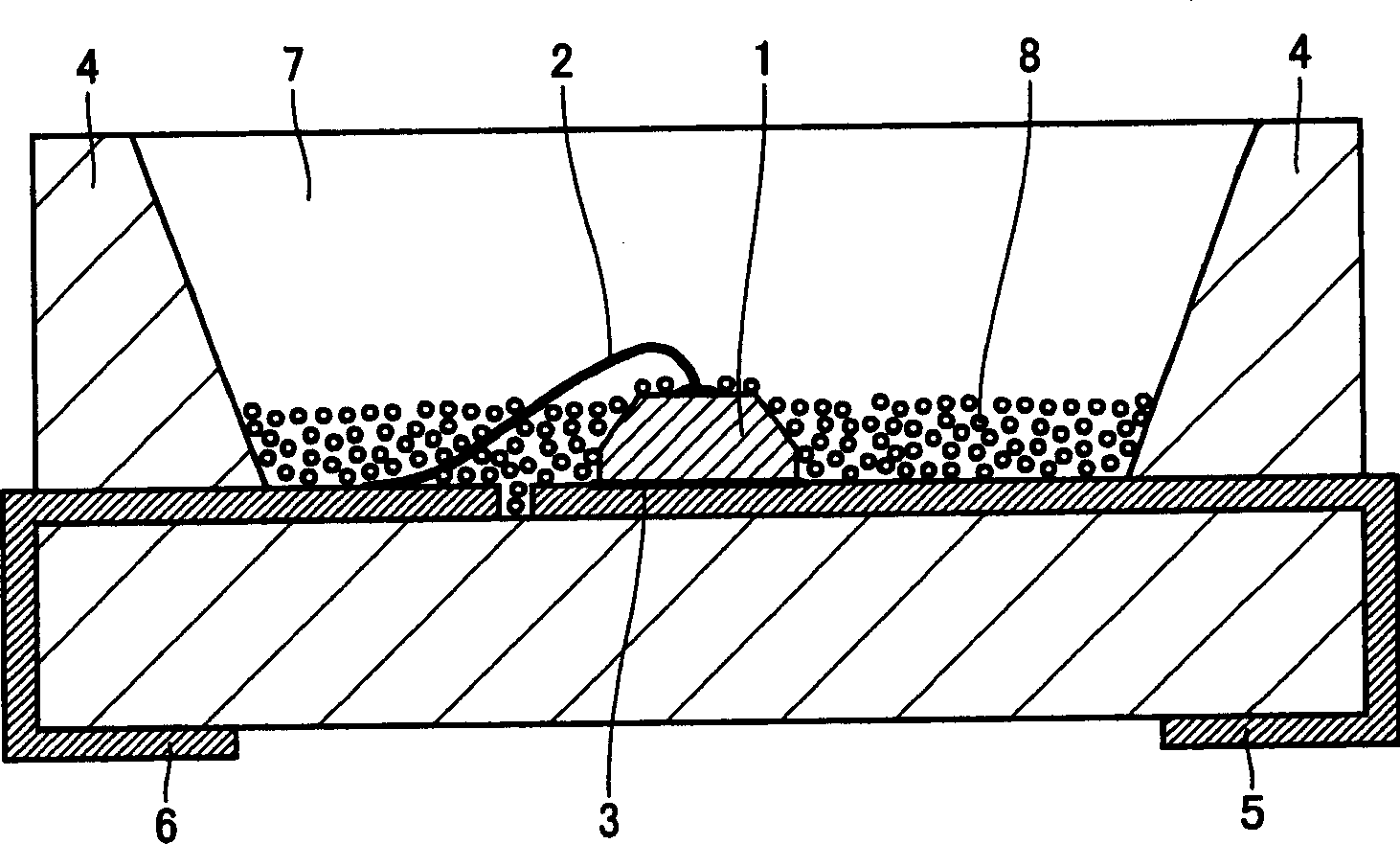
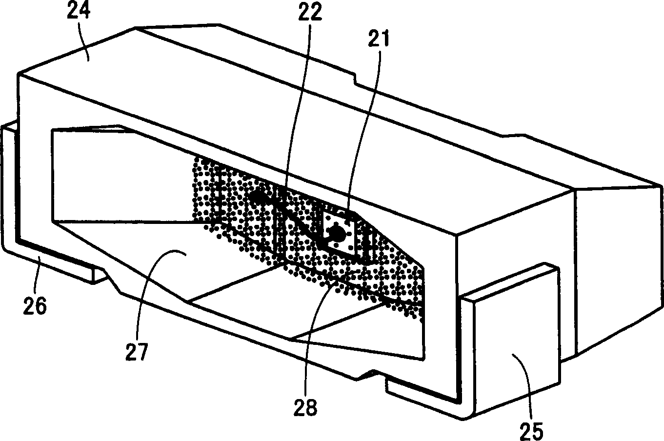
[0031] LED device

[0032] Figure 1A It is a perspective view of a surface mount type light emitting diode device as a typical example of the LED device of the present invention. Figure 1B is a cross-sectional view of the LED device. The device comprises positive and negative electrode pairs 5, 6 formed of metal plates, and a case 4 made of heat-resistant resin. The housing 4 can be formed by insert molding and takes the shape of a reflective cup. The LED substrate 1 has a side portion and a top portion, and a part of the side portion is a slope. The LED substrate 1 is electrically connected to the electrode 5 through the conductive material 3 in the housing 4 , and is electrically connected to the other electrode 6 through the metal wire 2 .

[0033] The casing 4 is sealed with a translucent resin 7, and near its bottom surface, a fluorescent material 8 having a substantially uniform thickness is provided in a layered form. The fluorescent material layer 8 is formed to...


PUM

PropertyMeasurementUnit
thicknessaaaaaaaaaa
sizeaaaaaaaaaa

Abstract

An LED device that is excellent in color mixture and small in variation of chromaticity is provided. The LED device includes, in a package, an LED chip, a fluorescent material excited by light from the LED chip to generate light with a wavelength different from that of the light from the LED chip, and a translucent resin holding the fluorescent material. The LED chip has a side-surface portion, a top-surface portion, a bottom-surface portion, and a light-emitting layer sandwiched between the top-surface portion and the bottom-surface portion, and the fluorescent material in the translucent resin is provided in a layer form on a bottom surface of the package to entirely or partially cover the side-surface portion of the LED chip.

Description

[0001] This application is based on Japanese Patent Application No. 2005-054141 filed with the Japan Patent Office on February 28, 2005, the entire content of which is incorporated herein by reference. technical field [0002] The present invention relates to light emitting diode devices used in applications such as backlighting of liquid crystal displays, switchboard meters, and indicator lights. In particular, the present invention relates to a white and intermediate color light emitting diode device and a method of manufacturing the same. Background technique [0003] Traditional light-emitting diodes (hereinafter referred to as "LEDs") have such Figure 10A and 10B The device structure shown in . Such as Figure 10A and 10B As shown in , the LED device includes in the housing 14: an LED substrate 11, a fluorescent material 18 that is excited by light from the LED substrate 11 to generate light of different wavelengths, and a translucent resin 17. The LED substrate 11 ...

Claims


Application Information

Patent Timeline
Patent Type & Authority Applications(China)
IPC IPC(8): H01L33/00C09K11/08H01L33/32H01L33/50H01L33/60
CPCG02F1/133603H01L33/20H01L33/508H01L2933/0041H01L2224/48091H01L2224/48247H01L2224/48257H01L2224/48465H01L2224/73265H01L2224/8592H01L2924/10157H01L2924/10155H01L2924/00014H01L2924/00
Inventor 鸭下昌一
Owner SHARP KK
Why Eureka
Try Eureka