Fault positioning method

A fault location and fault technology, applied in the direction of fault location, electronic circuit testing, measuring devices, etc., can solve the problems of high cost, high density and replacement of replacement parts

Inactive Publication Date: 2006-10-25
HUAWEI TECH CO LTD
View PDF0 Cites 24 Cited by
  • Summary
  • Abstract
  • Description
  • Claims
  • Application Information

AI Technical Summary

Problems solved by technology

[0006] 1. Engineering and technical personnel need a lot of experience in single-board maintenance. For the maintenance of high-complexity single-boards, it takes a long time to establish such experience;
[0007] 2. For a high-complexity single board, its density is high, and a large number of BGA (Ball Grid Array, ball grid array structure) packaging devices are used, resulting in strict restrictions on the number of disassembly and assembly of the device, and the device cannot be replaced at will. The cost of the device is very high, and if the trial fails, it will cause a lot of waste;
[0008] 3. Difficulty transferring experience

Method used


Image

  • Fault positioning method
  • Fault positioning method
  • Fault positioning method

Examples


Embodiment Construction

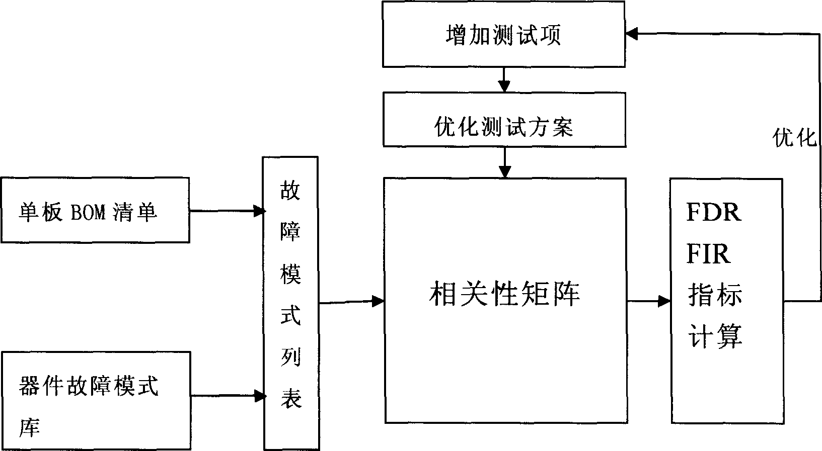
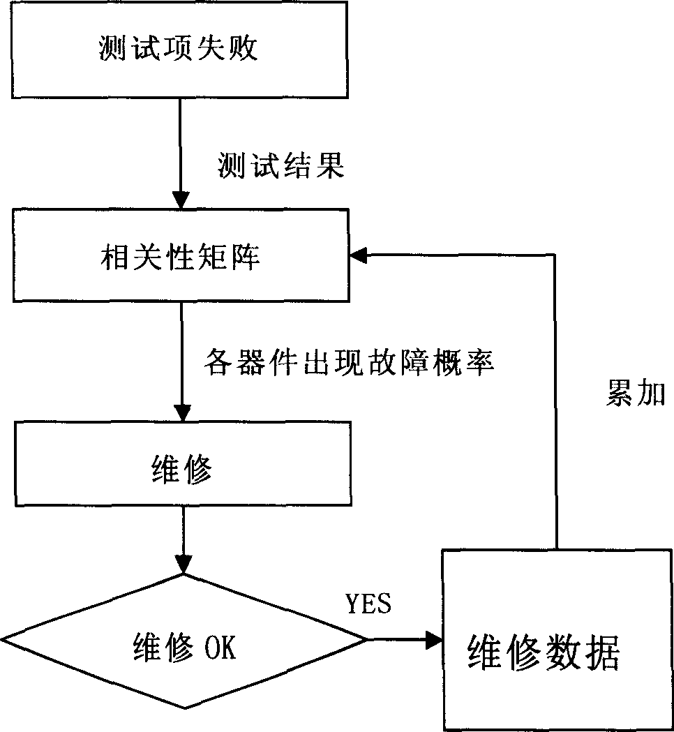
[0047] The present invention provides a fault location method, which can locate a specific device when a single board fails, and the method has the function of continuously correcting the location capability, such as Figure 4 As shown, the implementation of this method is as follows:

[0048] Step 1. For single board modeling, establish the corresponding relationship between failure modes and test items. The so-called failure mode refers to the possible failure of each device on the board, using the following correlation matrix form:

[0049]

[0050] Among them, the i-th row matrix Fi is:

[0051] [di1 di2… dij]

[0052] Indicates the correlation between the failure mode Fi and each test item, which indicates which test items fail when the device fails;

[0053] The failure mode Fi is established as follows:

[0054] (1.1) Obtain the device failure mode library, which contains all devices and all failure modes of the device;

[0055] (1.2) Obtain the device l...


PUM


Abstract

A fault location method includes steps: 1, establishing correlation matrix between fault pattern and tested item, 2, optimizing correlation matrix through fault location rate FDR and failure isolation rate FIR, 3, optimizing correlation matrix through maintenance data, 4, when single board gone wrong, according to optimized correlation matrix positioning fault device. Said invention utilizes Bayes' theorem to calculate single board fault probability and determining replacing which device according to probability to realize fault positioning. Said invented method has continuously modification positioning function.

Description

Technical field [0001] The invention relates to the testing field of circuit boards, in particular to a fault location method for devices on the circuit board. Background technique [0002] In the field of circuit board production and testing, circuit board defects are mainly divided into two categories, one is process defects, that is, short circuit, open circuit, and adjustment defects of circuit board components generated during processing. This type of defect , Usually use process testing methods, such as AOI (Automated Optical Inspection, automatic optical inspection), AXI (Automated X-ray Inspection, automatic X-ray inspection), ICT (In-Circuit Test, online testing), etc. for coverage. Another type of defect of the circuit board is the performance defect of the device, such as the damage of the internal storage unit of the memory. This type of defect can usually only be covered by an FT (Function Test) test. Using process testing, you can clearly know which device and pin h...

Claims


Application Information

Patent Timeline
Patent Type & Authority Applications(China)
IPC IPC(8): G01R31/28G01R31/00G01R31/02G01R31/08
Inventor 吴祥
Owner HUAWEI TECH CO LTD
Why Eureka
Try Eureka