Semiconductor acceleration sensor device and fabrication method thereof
一种加速度传感器、半导体的技术,应用在半导体器件、测量加速度、速度/加速度/冲击测量等方向,能够解决不能高精度检测加速度等问题,达到抑制畸变、检测精度提高的效果
- Summary
- Abstract
- Description
- Claims
- Application Information
AI Technical Summary
Problems solved by technology
Method used
Image

Examples
Embodiment approach 1
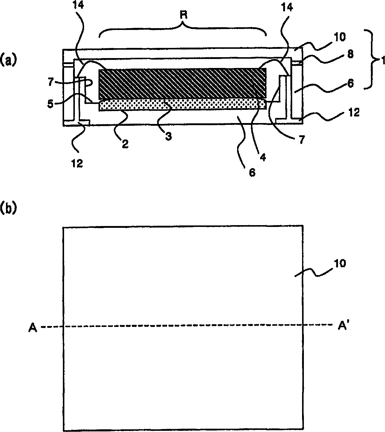
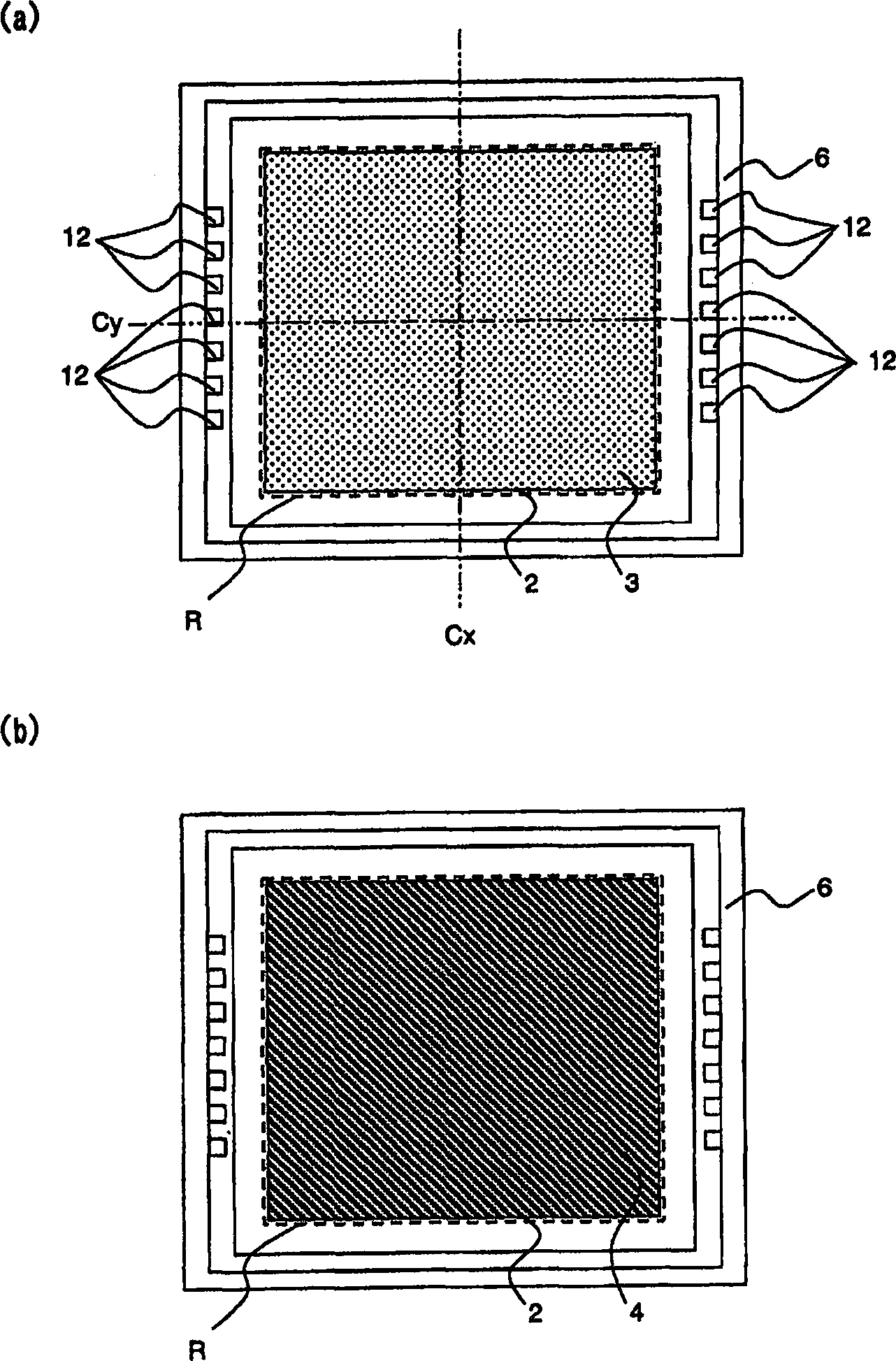
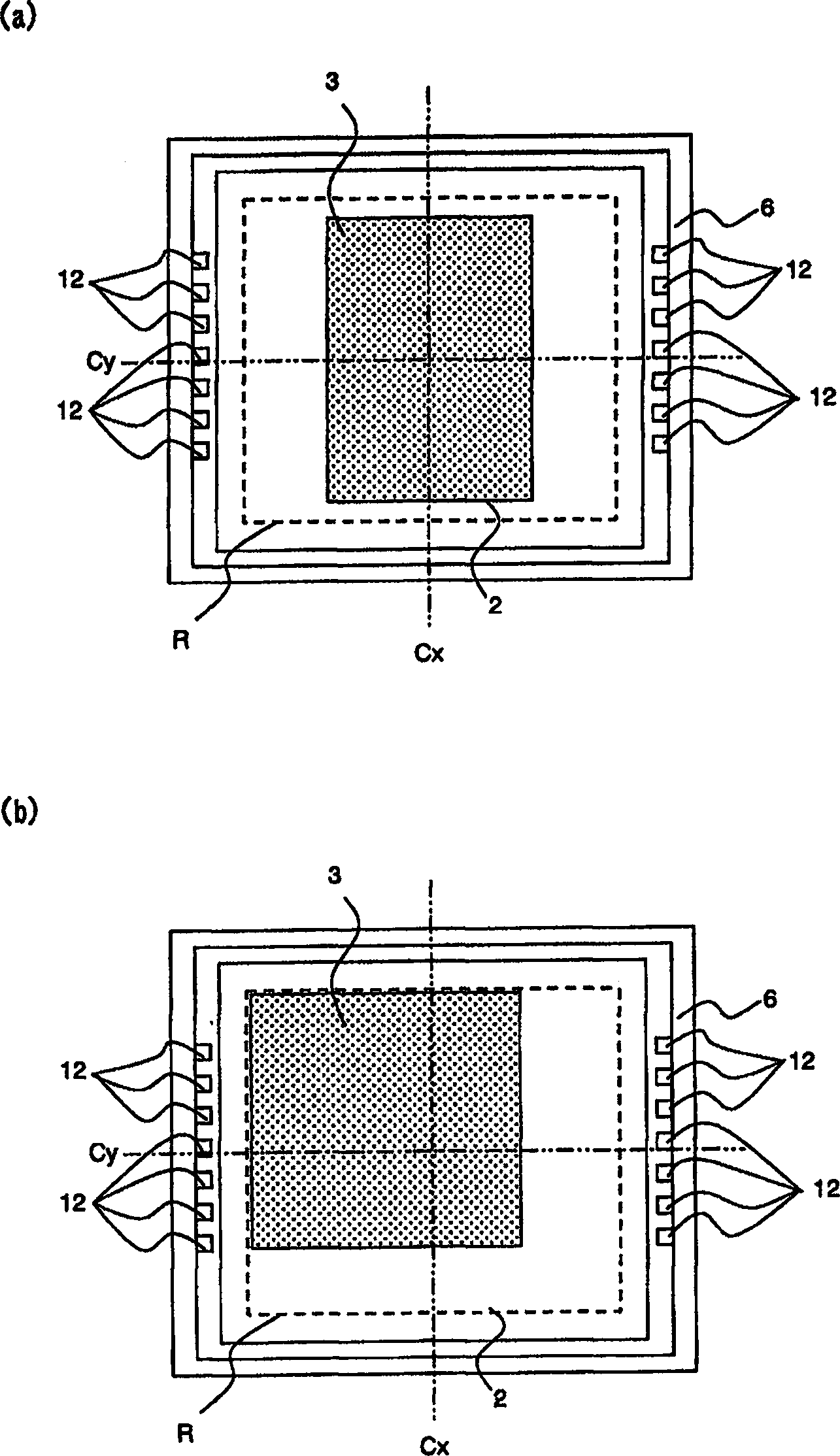
[0053] Use below Figure 1 to Figure 4 The structure and manufacturing method of the semiconductor acceleration sensor device according to Embodiment 1 of the present invention will be described. figure 1 (b) is a plan view of the semiconductor acceleration sensor device of this embodiment. figure 1 (a) is a cross-sectional view of the semiconductor acceleration sensor device of the present embodiment, and is figure 1 Sectional view of part A-A' of (b). figure 2 (a) is a plan view of the semiconductor acceleration sensor device according to this embodiment in a state where the upper cover 10 , the adhesive 8 , the wires 14 , and the acceleration sensor chip 4 are removed. figure 2 (b) for the figure 2 (a) is a plan view of a state where the acceleration sensor chip 4 is placed on the low elastic member 3 . image 3 is the shape, size or position of the low elastic member 3 and figure 2 (a) An example of a case where the low elastic member 3 shown in (a) is differen...
Embodiment approach 2
[0111] Use below Figure 7 to Figure 9 and Figure 4 The structure and manufacturing method of the semiconductor acceleration sensor device according to Embodiment 2 of the present invention will be described. In addition, the description of the same parts as the configuration and manufacturing method of the semiconductor acceleration sensor device according to Embodiment 1 will be omitted.
[0112] [structure]
[0113] Figure 7 (b) is a plan view of the semiconductor acceleration sensor device of this embodiment. Figure 7 (a) is a cross-sectional view of the semiconductor acceleration sensor device of the present embodiment, and is Figure 7 Sectional view of part A-A' of (b). Figure 8 (a) is a plan view of the semiconductor acceleration sensor device according to this embodiment in a state where the upper cover 10 , the adhesive 8 , the wires 14 , and the acceleration sensor chip 4 are removed. Figure 8 (b) is in Figure 8 (a) is a plan view of a state where the acc...
Embodiment approach 3
[0129] Use below Figure 10 to Figure 12 and Figure 4 The structure and manufacturing method of the semiconductor acceleration sensor device according to Embodiment 3 of the present invention will be described. In addition, the description of the same parts as the configuration and manufacturing method of the semiconductor acceleration sensor device according to Embodiment 1 will be omitted.
[0130] [structure]
[0131] Figure 10 (b) is a plan view of the semiconductor acceleration sensor device of this embodiment. Figure 10 (a) is a cross-sectional view of the semiconductor acceleration sensor device of the present embodiment, and is Figure 10 Sectional view of part A-A' of (b). Figure 11 (a) is a plan view of the semiconductor acceleration sensor device according to this embodiment in a state where the upper cover 10 , the adhesive 8 , the wires 14 , and the acceleration sensor chip 4 are removed. Figure 11 (b) is in Figure 11 (a) is a plan view of a state whe...
PUM
 Abstract
Description
Claims
Application Information
 - Generate Ideas
- Intellectual Property
- Life Sciences
- Materials
- Tech Scout
- Unparalleled Data Quality
- Higher Quality Content
- 60% Fewer Hallucinations
Browse by: Latest US Patents, China's latest patents, Technical Efficacy Thesaurus, Application Domain, Technology Topic, Popular Technical Reports.
© 2025 PatSnap. All rights reserved.Legal|Privacy policy|Modern Slavery Act Transparency Statement|Sitemap|About US| Contact US: help@patsnap.com