

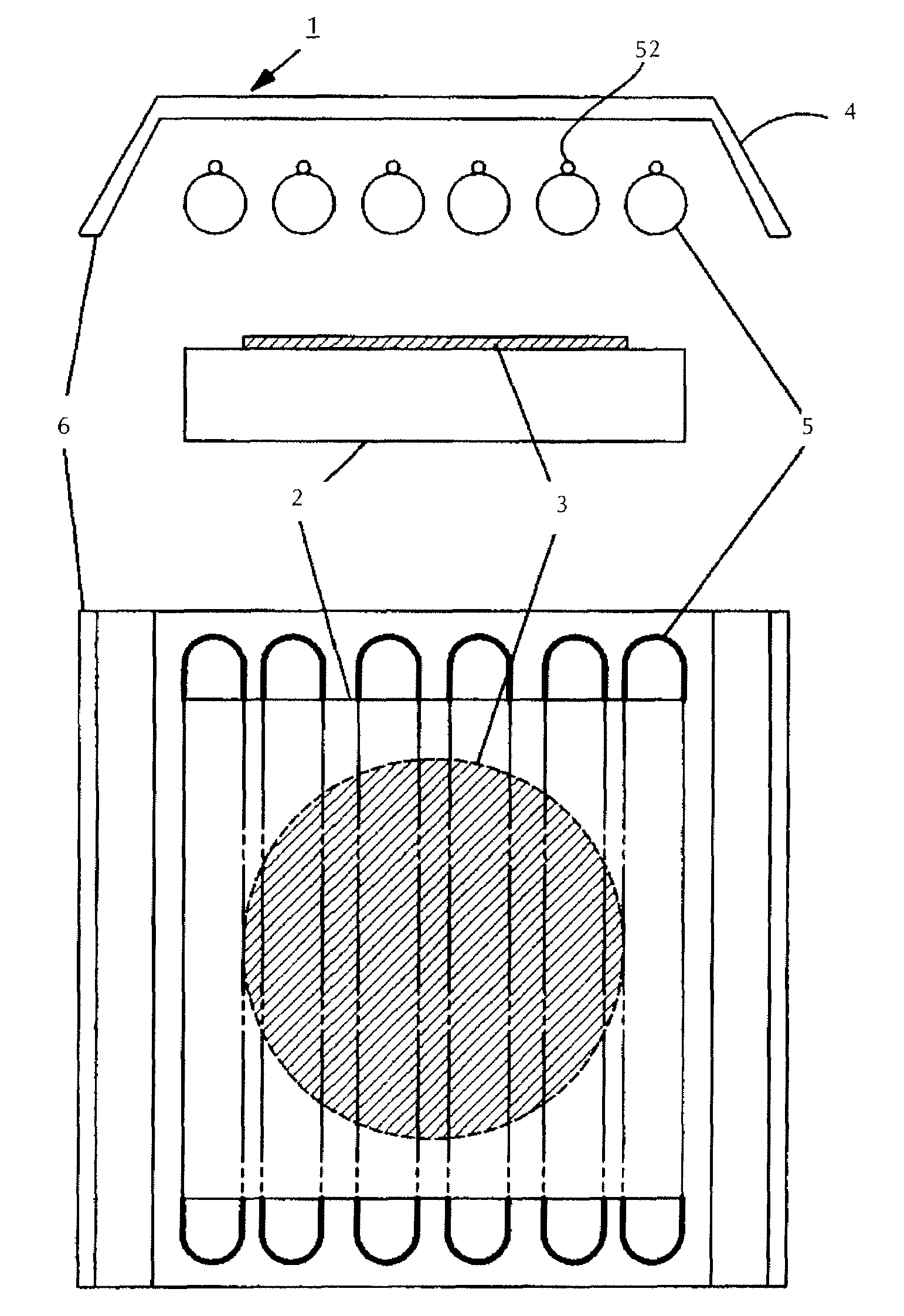
Substrate heating device and substrate heating method
a heating device and substrate technology, applied in the direction of gas-filled discharge tubes, transit-time tubes, chemical vapor deposition coatings, etc., can solve the problems of deformation or cracking, deformation or cracking by thermal strain on the substrate, abrupt rise in the temperature of the substrate, etc., to suppress the distortion or breaking of the substrate
- Summary
- Abstract
- Description
- Claims
- Application Information
AI Technical Summary
Benefits of technology
Problems solved by technology
Method used
Image

Examples
first embodiment
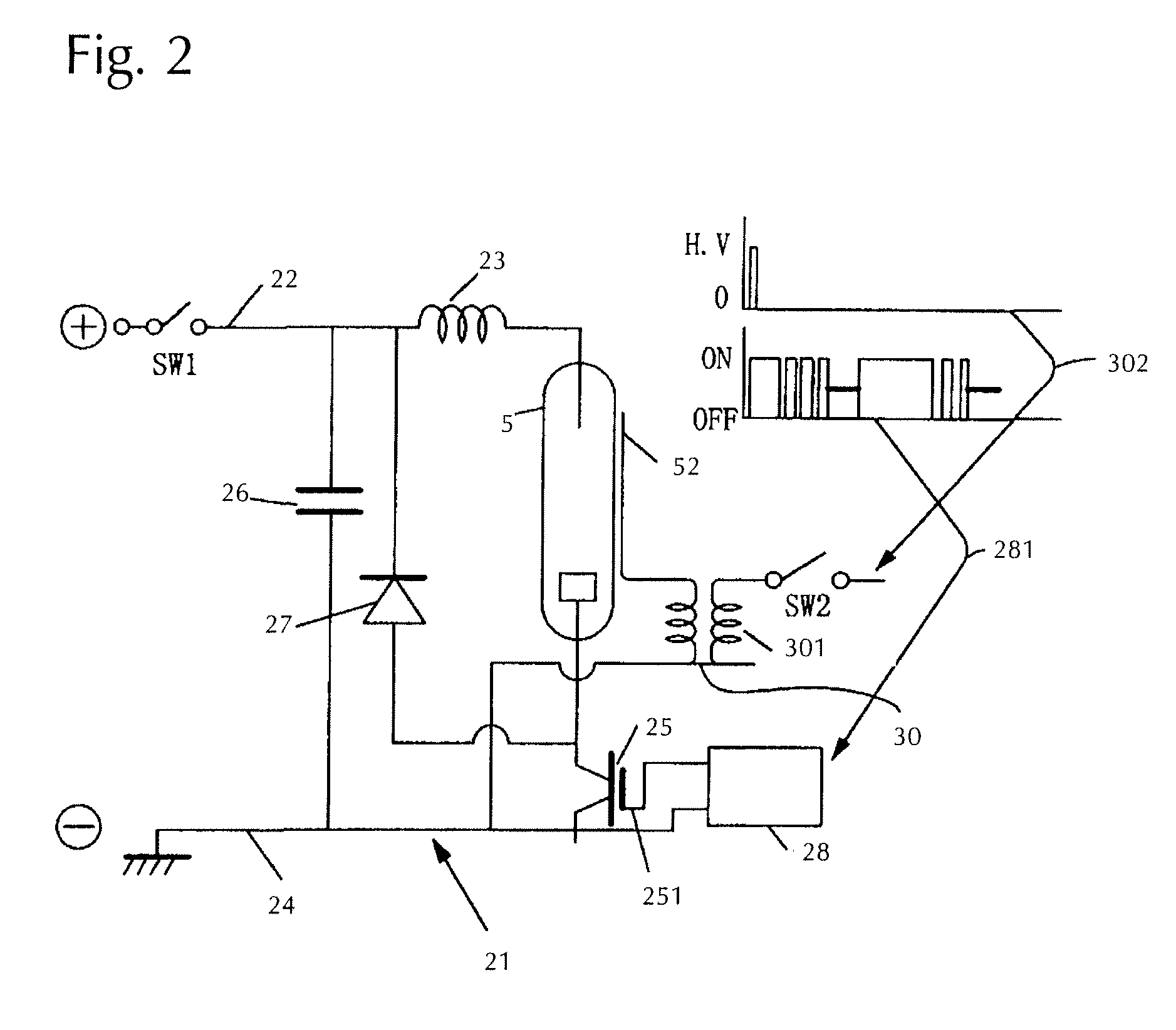
[0080]FIG. 5 is a graph of the timing of the temperature-rising pattern in the present invention, and shows a case where the first drive signal is composed of a drive signal that allows the first drive signal to be ON, for example, for 40 μsec, for the purpose of forming an arc discharge throughout the entire tube axis direction, and another drive signal that repeats on and off with a certain duty cycle, the second drive signal being composed of an on-signal that continues for a certain period of time.
[0081]The graph of FIG. 5 shows, respectively from the top: (I) the relationship between temperature and time of the topmost surface of the semiconductor wafer 3; (II) the gate signal to be input into the IGBT element; (III) the input timing of the trigger signal for illuminating the flash lamp 5; (IV) the charge-initiating signal to the charging capacitor to supply power to the flash lamp 5; (V) the lamp voltage of the flash lamp 5; and (VI) the lamp current of the flash lamp 5. The h...
second embodiment
[0096]FIG. 6 shows another temperature elevation pattern in accordance with the present invention. The parts (I) to (V) correspond to the same parts as in FIG. 5, and show the relationship between temperature and time of the topmost surface of the semiconductor wafer 3, the gate signal to be input to the IGBT element, the input timing of the trigger signal, a charging-initiating signal to the charging capacitor, the lamp voltage and the lamp current, respectively.
[0097]FIG. 6 is the same as FIG. 5 until the point of time c when the trigger signal of the flash lamp 5 is input. The pulse width to be input first as a gate signal of the IGBT element 25 is 40 μsec, similar to FIG. 5.
[0098]Subsequently, in this embodiment, until the topmost surface temperature of the semiconductor wafer 3 reaches 800° C., the IGBT element 25 is driven by the first drive signal, and the lamp is lit by switching the gate signal on and off for 10 μsec each. In addition, after that, the lamp is lit by switchi...
third embodiment
[0100]FIG. 7 shows another temperature elevation pattern in accordance with the present invention, and parts (I) to (VI) are the same as in FIG. 5, indicating the relationship between temperature and time of the topmost surface of the semiconductor wafer 3, the gate signal to be input to the IGBT element, the input timing of the trigger signal, a charging-initiating signal to the charging capacitor, the lamp voltage and the lamp current, respectively.
[0101]FIG. 7 is also the same as FIG. 5 until the point of time c when the trigger signal of the flash lamp 5 is input.
[0102]In addition, the IGBT element 25 is driven by the first drive signal, and in this embodiment, the pulse width to be input first as a gate signal of the IGBT element 25 is 40 μsec as similar to FIGS. 5 & 6. However, switching the gate signal of the IGBT element 25 to be input is turned on for 10 μsec, off for 10 μsec, on for 20 μsec and off for 10 μsec, and this enables the surface temperature of the topmost surfac...
PUM
| Property | Measurement | Unit |
|---|---|---|
| temperature | aaaaa | aaaaa |
| depth | aaaaa | aaaaa |
| depth | aaaaa | aaaaa |
Abstract
Description
Claims
Application Information