Mask for continuously transverse solidifying technology and method for forming polycrystal silicon layer

A technology of lateral solidification and polysilicon thin film, which is applied in the field of masks and can solve problems such as poor electrical properties

Active Publication Date: 2007-01-10
AU OPTRONICS CORP
View PDF0 Cites 4 Cited by
  • Summary
  • Abstract
  • Description
  • Claims
  • Application Information

AI Technical Summary

Problems solved by technology

According to the experimental results, the channel of the thin film transistor can have better electrical performance when the channel is parallel to the grain growth direction. On the contrary, if the channel of the tr

Method used


Image

  • Mask for continuously transverse solidifying technology and method for forming polycrystal silicon layer
  • Mask for continuously transverse solidifying technology and method for forming polycrystal silicon layer
  • Mask for continuously transverse solidifying technology and method for forming polycrystal silicon layer

Examples


Embodiment Construction

[0039] The invention discloses a mask applied to continuous lateral solidification (SLS) to produce a polysilicon film with dispersed crystal boundaries. The mask of the present invention will be described in detail below with reference to the accompanying drawings and multiple specific embodiments.

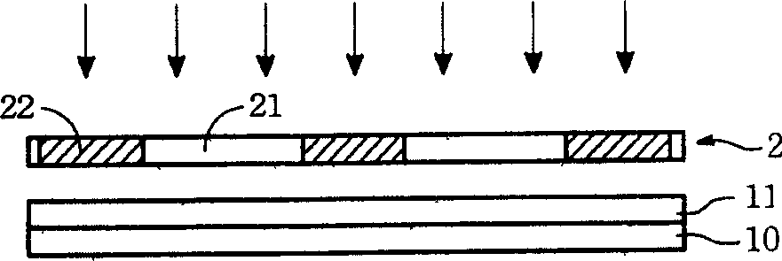
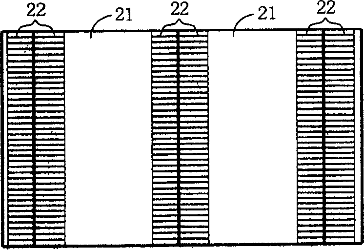
[0040] Such as figure 2 Shown is a schematic top view of a mask in a preferred embodiment of the present invention. figure 2 The mask 3 includes at least: a first area 31 , a second area 32 , and a third area 33 . Wherein, the first area 31 and the third area 33 are light-transmitting, and the second area 32 is light-shielding.

[0041] The first region 31 surrounds the second region 32 , and the first region 31 and the second region 32 have substantially the same peripheral shape. The third region 33 has the same peripheral shape as the first region 31 , and in this embodiment, the peripheral shapes of the above three regions are rectangular structures. Moreover, the third...


PUM


Abstract

The present invention disclose a mask used in continue transverse direction solidifying technology for generating one crystallizing boundary dispersive polysilicon film. The present invention mask at least contains one first zone, one second zone, and one third zone, wherein first zone and third zone being transparent, second zone being shading, first zone surrounded in second zone and first and second zone having basically same periphery shape, third zone and first zone having same periphery shape, and third zone and first zone and second zone parallel configured in one predetermined direction. Said invention has advantages of utilizing mask pattern complemental concept, designing out at least two crystal grain directional polysilicon pattern, through controlling mask plurality of shading zone and photic zone pattern area size to obtain perfect grain boundary.

Description

technical field [0001] The invention relates to a mask used in polysilicon thin film technology, in particular to a mask for producing a polysilicon thin film with dispersed crystal boundaries by continuous lateral solidification technology, specifically a mask and the formed polysilicon. Background technique [0002] Thin film transistors (Thin Film Transistor; TFT) have been widely used in active liquid crystal displays, and the materials used in the thin film transistors generally include amorphous silicon (amorphous-silicon) and polysilicon (poly-silicon). [0003] In the manufacture of liquid crystal displays, polycrystalline silicon materials have many characteristics superior to amorphous silicon materials. For example, polysilicon has larger grains, and electrons are easy to move freely in polysilicon, so the electron mobility (mobility) of polysilicon is higher than that of amorphous silicon. The response time of polysilicon thin film transistors made of polysilico...

Claims


Application Information

Patent Timeline
IPC IPC(8): G03F1/08G03F1/00G03F7/00H01L21/027G03F1/32
Inventor 赵志伟
Owner AU OPTRONICS CORP
Why Eureka
Try Eureka