

Method for testing GaN single-crystal fault kind and density
A technology of defect types and detection methods, which is applied in the directions of measuring devices, semiconductor/solid-state device testing/measurement, and material analysis through optical means, and can solve the requirements of electrical conductivity, long selection and scanning time, limited needle tip effect, etc. problem, to achieve the effect of wide applicability
- Summary
- Abstract
- Description
- Claims
- Application Information
AI Technical Summary
Problems solved by technology
Method used
Image

Examples
Embodiment Construction
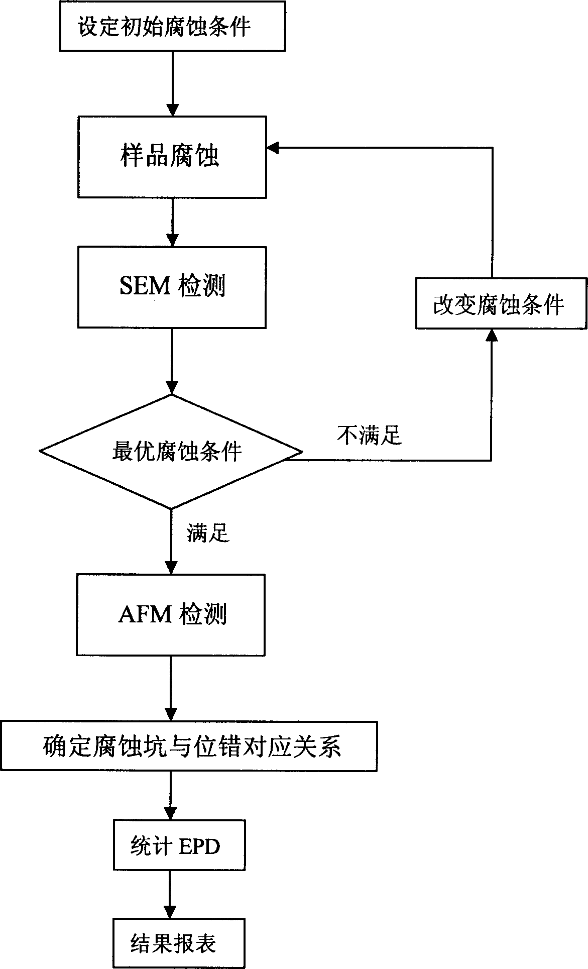
[0033] refer to figure 1 , which is a block flow diagram of the detection method of the present invention, from which the specific steps of the method can be clearly seen. Now combine specific steps and specific examples to illustrate its working process:
[0034] 1. Set the initial corrosion conditions. The initial corrosion temperature and time were estimated from the surface topography of the uncorroded sample.
[0035] 2. Sample corrosion. Clean and remove the organic contamination on the surface of the GaN sample, preheat the crucible to remove the water in it, add KOH particles to heat to the set temperature, put the sample and time it, take out the sample and clean it after the set time. The residual potassium hydroxide is discharged after treatment, and the crucible is cleaned for the next use.
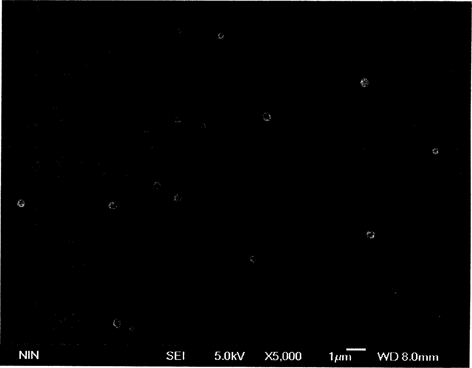
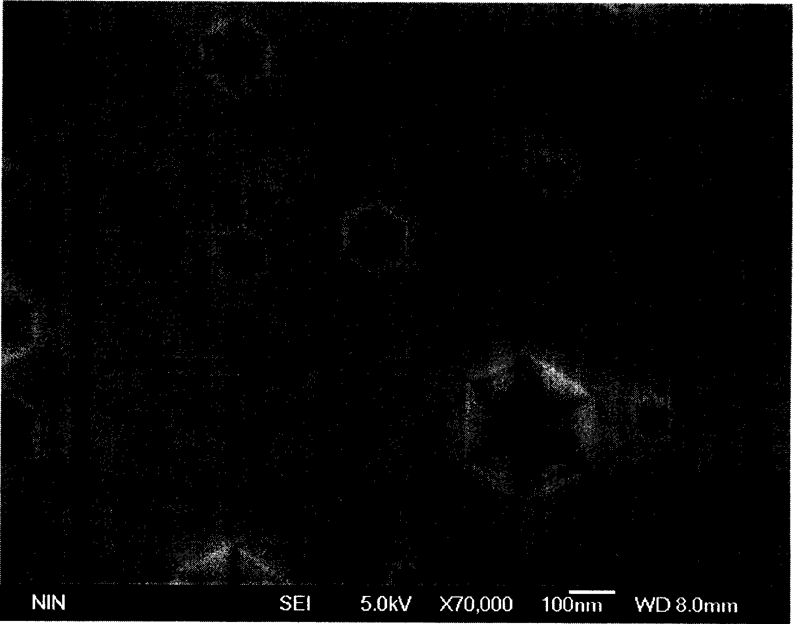
[0036] 3. Carry out SEM detection. On the corroded sample, select nine positions on a wafer or semi-circle, and select more than 3 microscopic areas near each position to...
PUM
 Abstract
Description
Claims
Application Information