Electron emitting element

A technology of electron emission and electron injection, which is applied in the direction of electrical components, discharge tube/lamp components, circuits, etc., can solve the problems of fluctuations in electron emission characteristics, small electric field concentration, and small emitted electron energy, so as to improve linear transmission performance, reduce power consumption, and reduce intermodulation distortion

Inactive Publication Date: 2007-01-17
NGK INSULATORS LTD
View PDF4 Cites 0 Cited by
  • Summary
  • Abstract
  • Description
  • Claims
  • Application Information

AI Technical Summary

Problems solved by technology

[0003] Conventional examples of such electron emission elements include, for example, Patent Documents 1 to 5, but they have the following problems: because none of them use a dielectric in the emitter portion, forming or micromachining is required between opposing electrodes, and for electron emission High voltage must be applied for emission, and the panel manufacturing process is complicated and the manufacturing cost is high
[0014] However, since the edge portion of the u

Method used


Image

  • Electron emitting element
  • Electron emitting element
  • Electron emitting element

Examples


Embodiment Construction

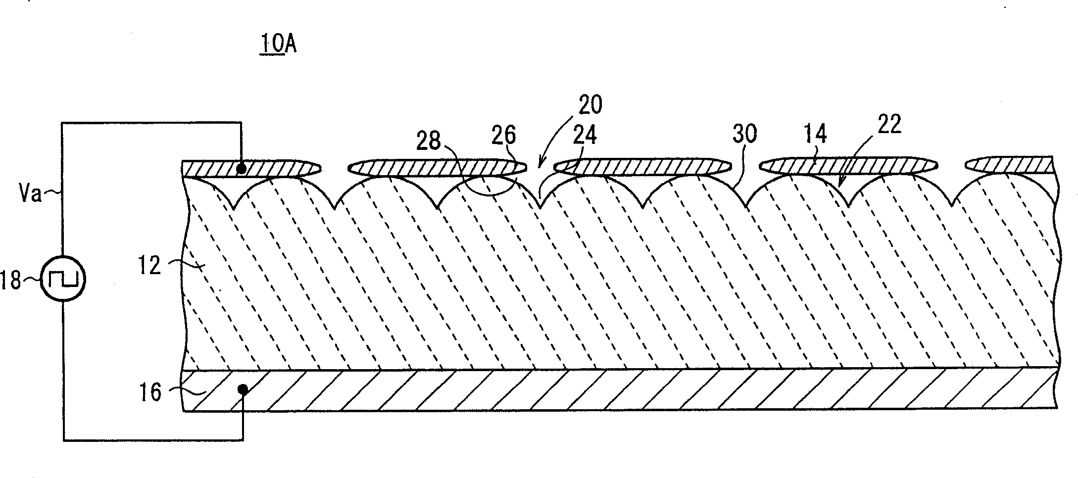
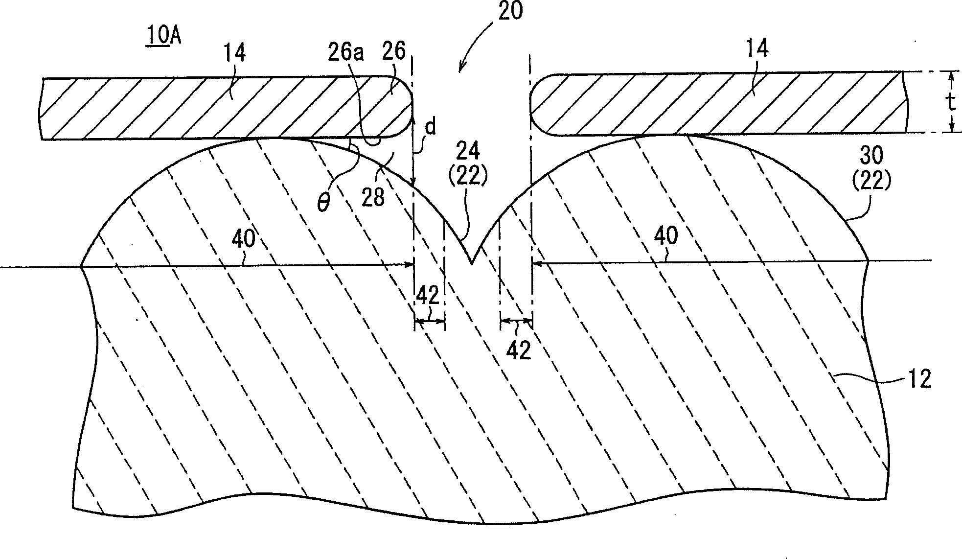
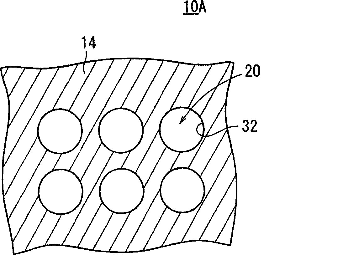
[0089] Below, refer to Figure 1 to Figure 52 Embodiments of the electron emission element of the present invention will be described.

[0090] First, the electron emission element of this embodiment can be used in electron beam irradiation devices, light sources, alternative LEDs, electronic component manufacturing devices, and circuit components in addition to the use as a display.

[0091] The electron beam of the electron beam irradiation device is superior in absorption property in terms of high energy, compared with the ultraviolet rays of the currently popular ultraviolet irradiation device. As an example of application, in semiconductor devices, it has the function of curing the insulating film when stacking wafers; in printing and drying, it has the function of hardening printing ink without spots; and in the state of sterilizing medical devices in the state of packaging them as they are. effect.

[0092] As a light source application, it is suitable for high bright...


PUM


Abstract

An electron emitting element (10A) is provided with an emitter part (12) composed of a dielectric material, and an upper electrode (14) and a lower electrode (16) whereupon a driving voltage (Va) is applied for electron emission. The upper electrode (14) is formed on an upper plane of the emitter part (12), and the lower electrode (16) is formed on a lower plane of the emitter part (12). The upper electrode (14) is provided with a plurality of penetrating parts (20) from which the emitter part (12) is exposed. In the upper electrode (14), a plane facing the emitter part (12) at a circumference part (26) of the penetrating part (20) is separated from the emitter part (12).

Description

technical field [0001] The present invention relates to an electron emission element having a first electrode and a second electrode formed in an emitter portion. Background technique [0002] Currently, an electron emission element has a cathode electrode and an anode electrode, and is used in various applications such as a field emission display (FED) or a backlight. When used in an FED, a plurality of electron emission elements are arranged two-dimensionally, and a plurality of phosphors are respectively arranged to face these electron emission elements at predetermined intervals. [0003] Conventional examples of such electron emission elements include, for example, Patent Documents 1 to 5, but they have the following problems: because none of them use a dielectric in the emitter portion, forming or micromachining is required between opposing electrodes, and for electron emission High voltage must be applied for emission, and the panel manufacturing process is complicat...

Claims


Application Information

Patent Timeline
IPC IPC(8): H01J1/312
CPCB82Y10/00H01J2201/3125H01J31/127H01J63/02H01J1/312
Inventor 武内幸久七泷努大和田岩赤尾隆嘉
Owner NGK INSULATORS LTD
Why Eureka
Try Eureka