
Semiconductor device

A semiconductor and power system technology, applied in semiconductor devices, semiconductor/solid-state device manufacturing, electric solid-state devices, etc., can solve problems such as increasing chip size

Inactive Publication Date: 2010-06-16
ROHM CO LTD
View PDF6 Cites 0 Cited by
  • Summary
  • Abstract
  • Description
  • Claims
  • Application Information

AI Technical Summary

Problems solved by technology

Therefore, it is not enough for a semiconductor device to arrange ESD protection components for power supply only in the space where the components of internal circuits and input and output circuits are not arranged. space in the component part, therefore, will result in an increase in chip size

Method used


Image

  • Semiconductor device
  • Semiconductor device
  • Semiconductor device

Examples


Embodiment Construction

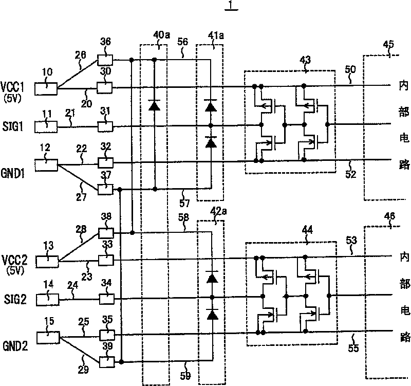
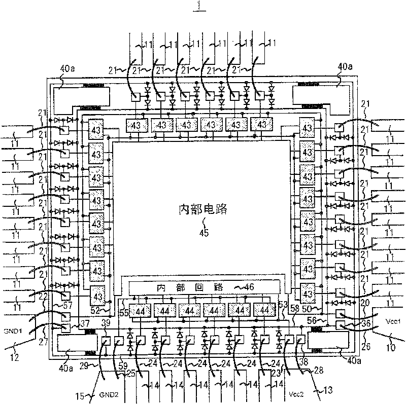
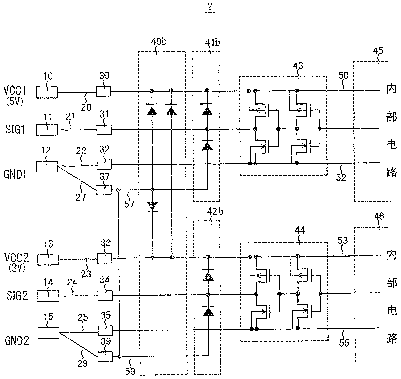
[0024] Hereinafter, the best mode for carrying out the present invention will be described with reference to the drawings. figure 1 It is a partial circuit diagram showing the connection state of each terminal in the semiconductor device according to the preferred first embodiment of the present invention. The semiconductor device 1 has two power supply systems of a 5V digital power supply system (first power supply system) and a 5V analog power supply system (second power supply system) as a plurality of power supply systems.

[0025] The first power supply system has a power supply (VCC1) terminal 10, a ground (GND1) terminal 12, and at least one signal (SIG1) terminal 11 for inputting and outputting signals with the outside. The second power supply system has a power supply (VCC2) terminal 13, a ground (GND2) terminal 15, and at least one signal (SIG2) terminal 14 for inputting and outputting signals with the outside. In addition, the first power supply system has a power...


PUM


Abstract

In a semiconductor device, ESD damage countermeasures are taken for a signal terminal of one power supply system, with a power supply (or grounding) terminal of other power supply system as a reference. The semiconductor device suppresses chip size increase caused by the countermeasures, while taking such countermeasures. The semiconductor device (1) is provided with ESD protection bonding pads (36-39) connected with the power supply terminals (10, 13) and grounding terminals (12, 15) with bonding wires (26-29) in the first and second power supply systems, ESD protection element parts (41a, 42a) for each signal, which are connected with signal bonding pads (31, 34) and the ESD protection bonding pads (36-39) to protect input / output circuits (43, 44), and a power supply ESD protection element part (40a), which is connected with the ESD protection bonding pads (36, 37).

Description

technical field [0001] The present invention relates to a semiconductor device having a plurality of power supply systems. Background technique [0002] Conventionally, a semiconductor device having a plurality of power supply systems, that is, a semiconductor device having a plurality of pairs of power supply terminals and ground terminal pairs, and a semiconductor device provided with semiconductor elements between each terminal pair, has been subjected to electrostatic discharge ( ESD) preventive measures are taken so that static electricity applied to signal terminals will not be destroyed by electrostatic discharge (ESD) even if it is discharged through any power supply terminal and ground terminal (for example, Patent Document 1). [0003] Figure 4 It is a partial circuit diagram showing the connection state of each terminal in a conventional semiconductor device having two power supply systems, a digital power supply system and an analog power supply system. The sem...

Claims


Application Information

Patent Timeline
Patent Type & Authority Patents(China)
IPC IPC(8): H01L21/822H01L21/82H01L27/04H01L27/02
CPCH01L27/0255H01L2924/3011H01L2224/48091H01L2224/49175H01L2224/05554H01L2924/13091H01L2924/00014H01L2924/00H01L27/04
Inventor 加藤工原英夫
Owner ROHM CO LTD
Features
  • Generate Ideas
  • Intellectual Property
  • Life Sciences
  • Materials
  • Tech Scout
  • Unparalleled Data Quality
  • Higher Quality Content
  • 60% Fewer Hallucinations
Learn More