Memory control apparatus

A control device and memory technology, applied in the direction of instruments, memory address/allocation/relocation, electrical digital data processing, etc., can solve the problems of data buffer hit rate reduction, data buffer hit, and failure to obtain external memory matching. , to achieve effective access and prevent the reduction of hit rate

Inactive Publication Date: 2007-03-21
PANASONIC CORP
View PDF1 Cites 6 Cited by
  • Summary
  • Abstract
  • Description
  • Claims
  • Application Information

AI Technical Summary

Problems solved by technology

[0006] In the device disclosed in the above publication, when the access from the main board is performed randomly, if a specific address as a part of the address of the data buffer is read, the data buffer must be invalidated. Hit rate reduction, deterioration of access efficiency to external memory issues
[0007] Moreover, when it is necessary to invalidate the data buffer, a method of issuing an access request to another address area on the external memory as a dummy access request has been previously performed, but there is a method for issuing a request to the external memory. Pro

Method used


Image

  • Memory control apparatus
  • Memory control apparatus
  • Memory control apparatus

Examples


no. 2 approach

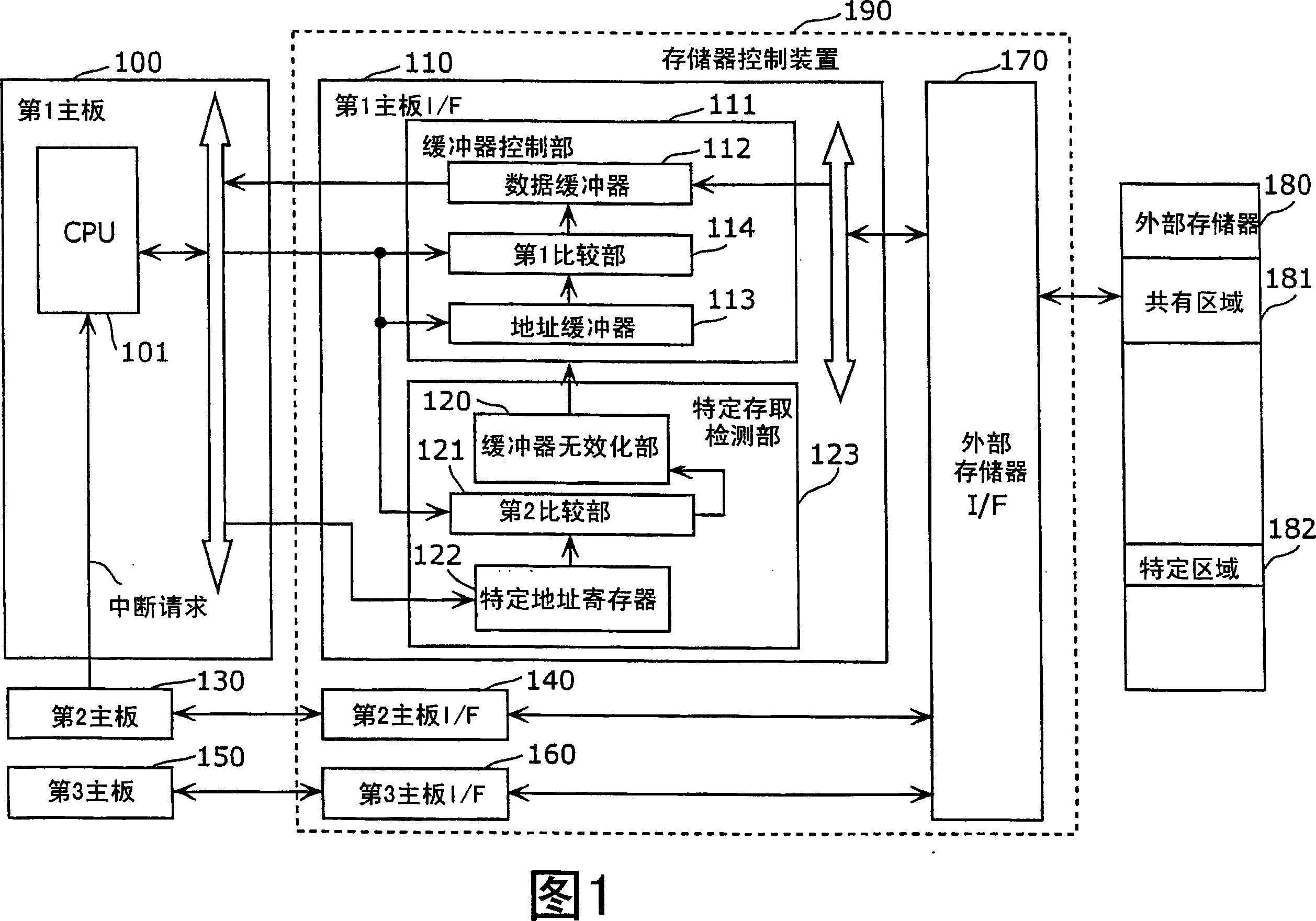
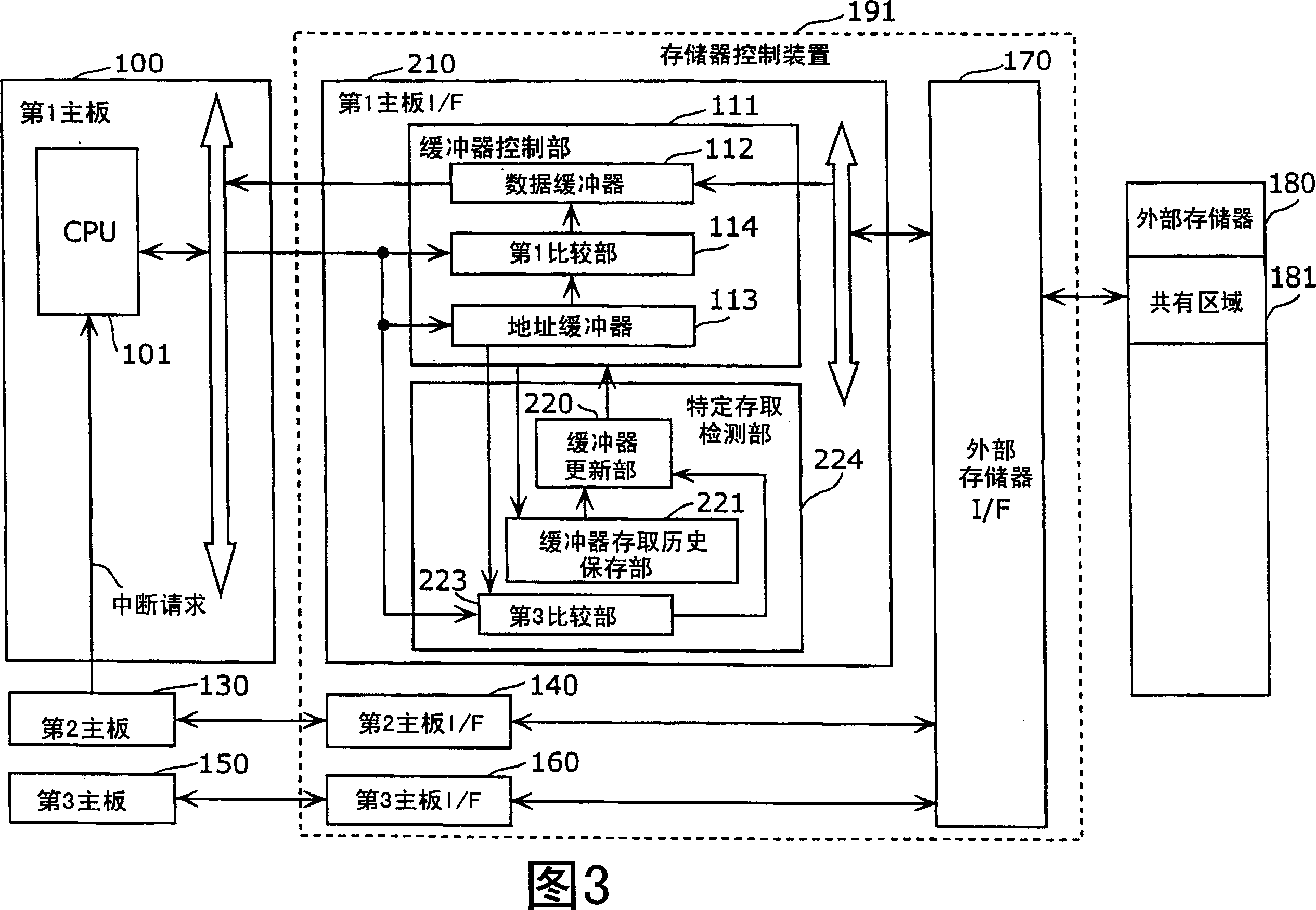
[0091] FIG. 3 is a block diagram showing an example of the functional configuration of the memory control device 191 of the second embodiment. In FIG. 3 , together with the memory control device 191 , the first motherboard 100 , the second motherboard 130 , the third motherboard 150 , and the external memory 180 are shown.

[0092] The memory control device 191 is configured by replacing the specific access detection unit 123 of the first motherboard I / F 110 of the memory control device 190 (see FIG. 1 ) described in the first embodiment with the specific access detection unit 224 . In FIG. 3 , the same function blocks as those of the access control device 190 are denoted by the same symbols, and description thereof will be omitted.

[0093] The specific access detection unit 224 is a unit that controls the buffer control unit 111 to forcibly access the external memory 180 every other time when consecutive access requests to the same address occur, and includes a buffer update...

no. 3 approach

[0116] FIG. 5 is a block diagram showing an example of the functional configuration of the memory control device 192 according to the third embodiment. In FIG. 5 , together with the memory control device 192 , the first motherboard 100 , the second motherboard 130 , the third motherboard 150 , and the external memory 180 are shown.

[0117] The memory control device 192 has a configuration in which the dummy access issuing unit 302 is added to the memory control device 190 (see FIG. 1 ) described in the first embodiment. In FIG. 5 , the same functional blocks as those of the memory control device 190 are assigned the same reference numerals, and description thereof will be omitted.

[0118] The dummy access issuing unit 302 receives an interrupt request from the second main board 130 indicating that the data in the common area 181 on the external memory 180 is updated, and issues an access to the above-mentioned specific address to the first main board I / F 110. requested unit...

no. 4 approach

[0129] Next, the configuration of the fourth embodiment will be described.

[0130] FIG. 7 is a block diagram showing an example of the functional configuration of the memory control device 193 according to the fourth embodiment. In FIG. 7 , the first main board 100 , the second main board 130 , the third main board 150 , and the external memory 180 are shown together with the memory control device 193 .

[0131] The memory control device 193 is configured by adding the dummy access issuing unit 402 to the memory control device 191 (see FIG. 3 ) described in the second embodiment. In FIG. 7 , the same blocks as those of the memory control device 191 are denoted by the same reference numerals, and description thereof will be omitted.

[0132] The dummy access issuing unit 402 is a unit that receives an interrupt request from the second main board 130 indicating that the data in the common area 181 on the external memory 180 has been updated, and issues an access request to the...


PUM


Abstract

To provide a memory control device capable of surely providing consistency to an external memory while suppressing degradation of access efficiency to the external memory. This memory control device is provided with: a data buffer 112 and an address buffer 113 holding data and an address related to an access request of the past from a first master 100; a first comparison part 113 for comparing, when receiving a new access request, its address with the address in the address buffer 113; a buffer control part 111 for issuing an access request to an external memory I/F 170 according to the comparison or outputting the data in the data buffer 112 to the first master 100; and a specific access detection part 123 for negating the content of the data buffer 112 regardless of the result of the comparison in detecting the access request to the specific address held in a specific address register 122.

Description

[0001] technology area [0002] The invention relates to a memory control device for sharing data on an external memory by a plurality of main boards and performing data transmission between the main board and the external memory. Background technique [0003] In the past, the following technology has been adopted in the memory control device, that is, when the access unit of the interface for accessing the external memory is larger than the access unit of the motherboard, in order to efficiently read the external memory, the external memory side is provided. In the data buffer corresponding to the access unit, the data of the data buffer unit is read and stored from the external memory in advance, and when read access (read access) in the unit address area occurs consecutively, the external memory is not accessed, but is read from the data buffer. Here, when a specific motherboard reads data on the external memory rewritten by other motherboards, the data buffer needs to be ...

Claims


Application Information

Patent Timeline
IPC IPC(8): G06F12/08
CPCG06F13/1631
Inventor 南木秀宪三野吉辉隅田圭三
Owner PANASONIC CORP
Why Eureka
Try Eureka