

Substrate processing unit and substrate processing apparatus
A substrate processing device and a substrate processing technology, which can be applied to devices for coating liquid on surfaces, electrical components, electrolysis processes, etc., and can solve problems such as difficulty in releasing substrates and deformation of substrates and substrates
- Summary
- Abstract
- Description
- Claims
- Application Information
AI Technical Summary
Problems solved by technology
Method used
Image

Examples
Embodiment Construction
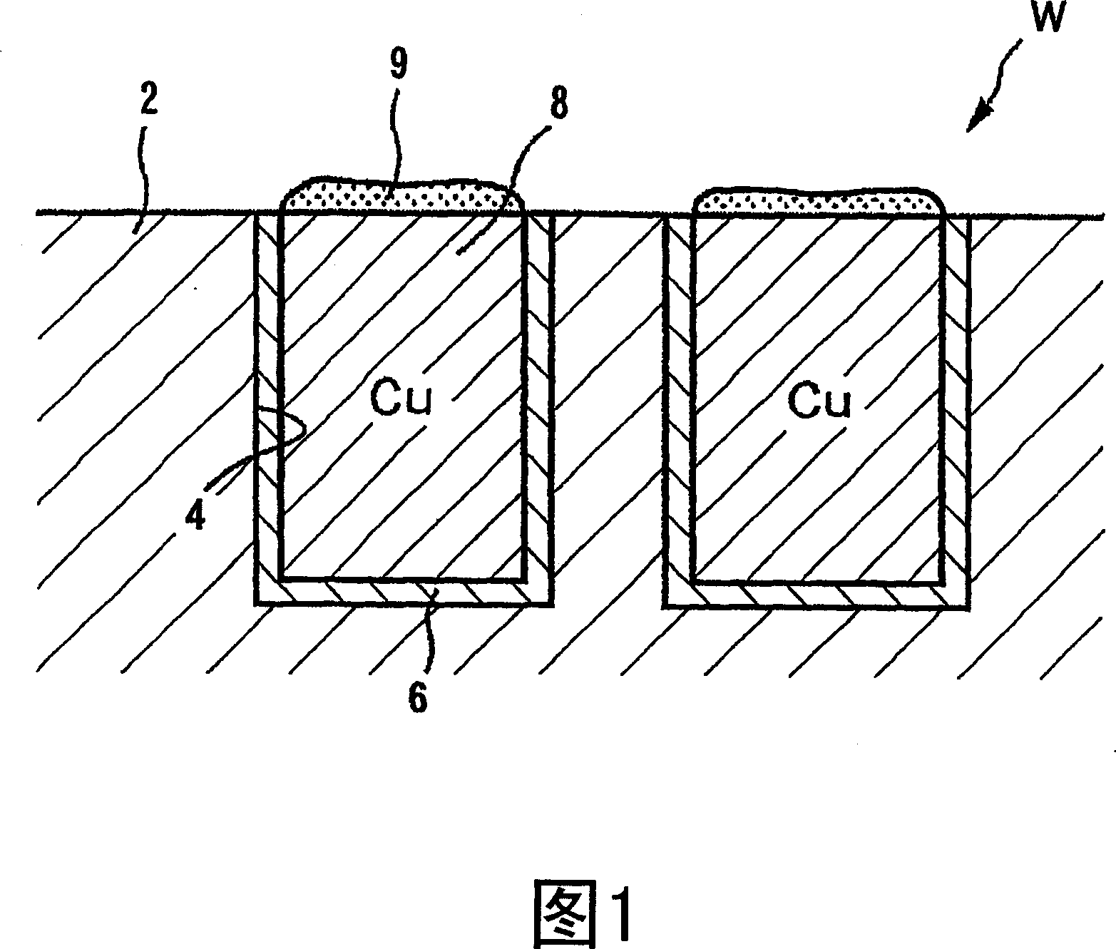
[0079] Embodiments of the present invention will be described below with reference to the drawings. This embodiment shows an example of application to an electroless plating apparatus capable of efficiently forming, for example, a protective film 9 (see FIG. 1 ) using electroless plating on the surface of wiring formed on a substrate. Of course, electrolytic plating equipment, CVD, and the like can also be applied to other substrate processing equipment.
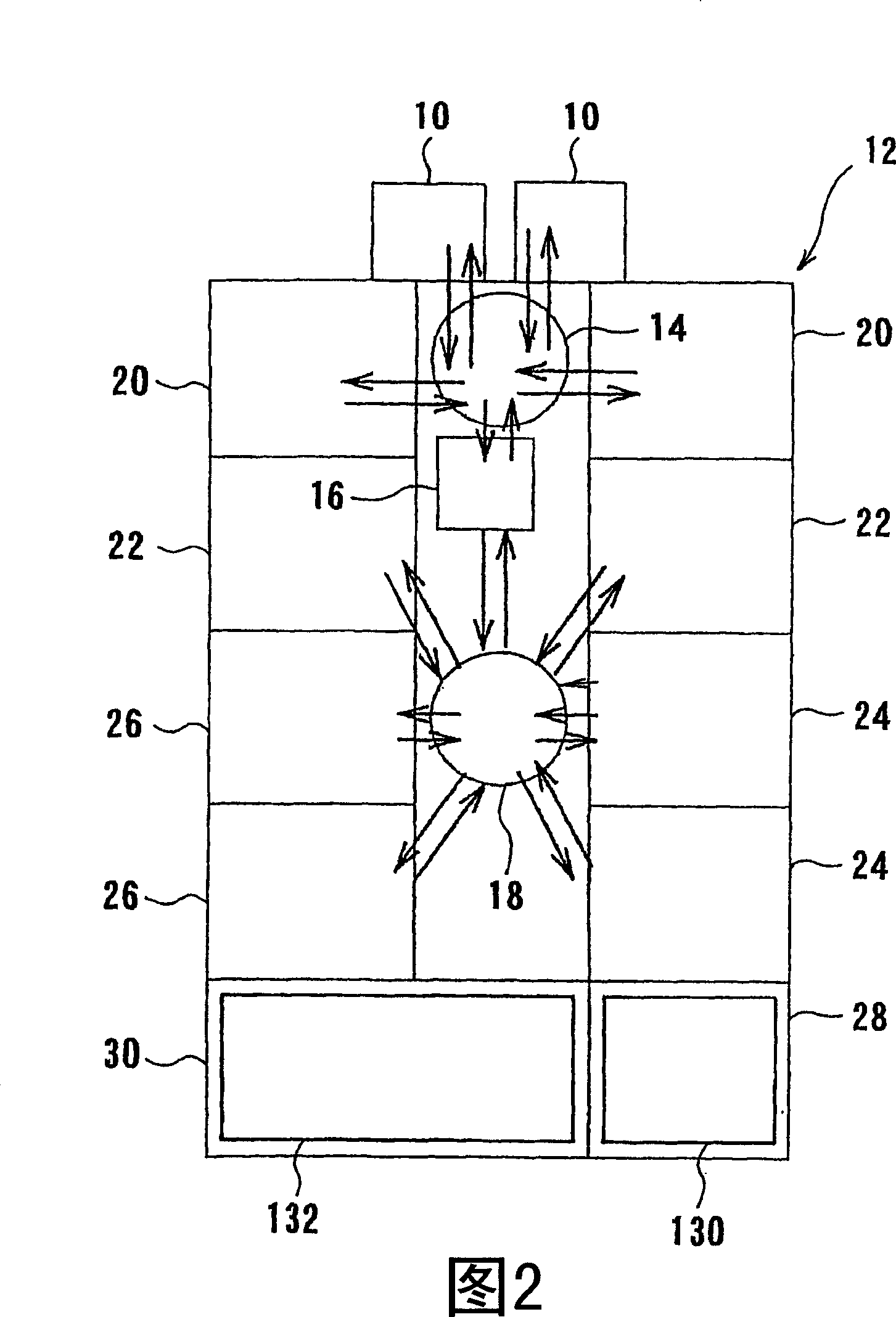
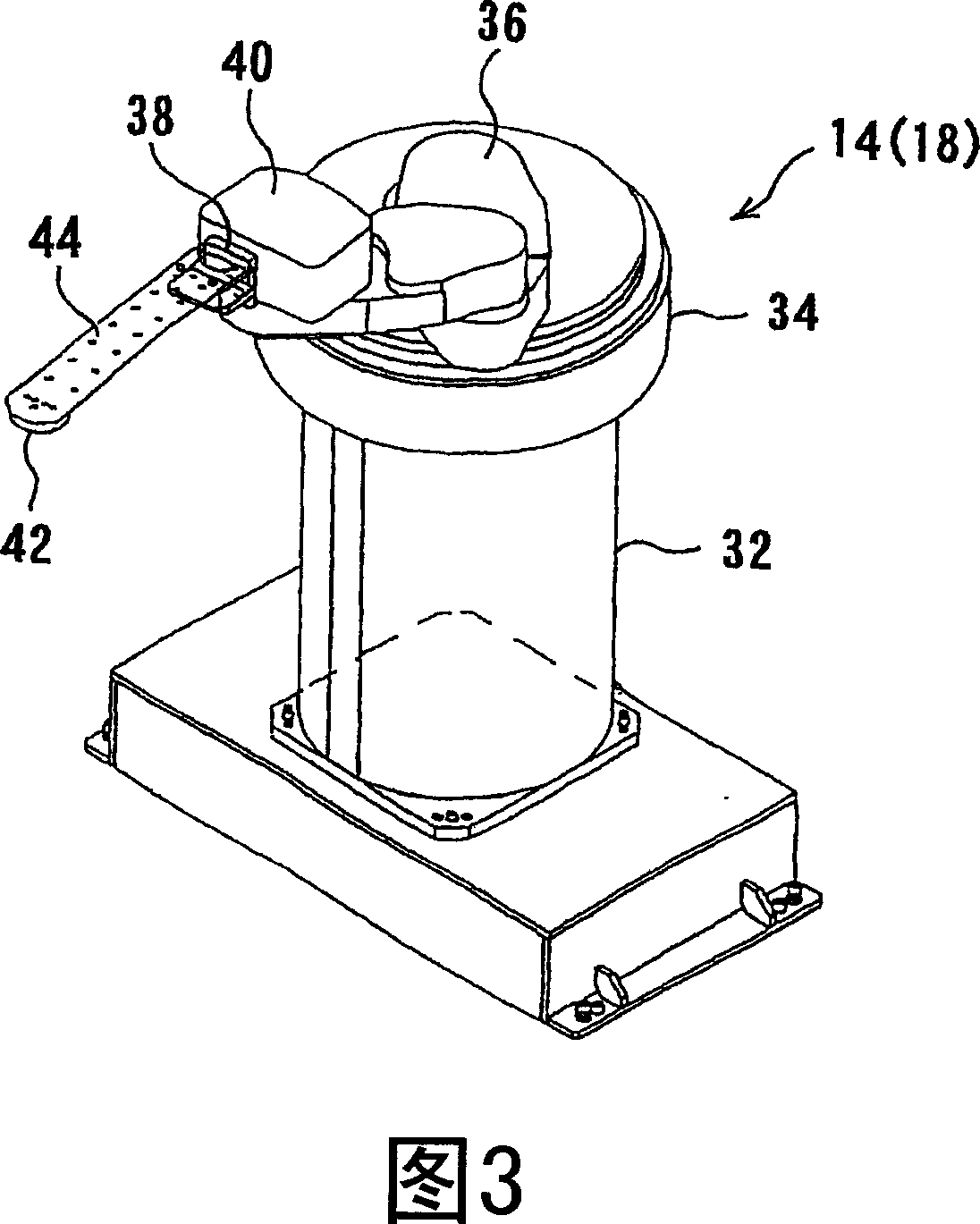
[0080]FIG. 2 is a plan view showing a substrate processing apparatus (electroless plating apparatus) according to an embodiment of the present invention. As shown in FIG. 2 , the substrate processing apparatus includes a rectangular apparatus frame 12 which is detachably detachable, for example, from a transport box 10 such as a SMIF box (sumifbox) that accommodates a plurality of substrates such as semiconductor wafers. Inside the apparatus frame 12, a first substrate transfer robot (robot) 14, a temporary placement table ...
PUM
 Abstract
Description
Claims
Application Information