Biosensor

A biosensor and substrate technology, applied in subcutaneous biometrics, biometric identification, instruments, etc., can solve the problems of capacitive fingerprint sensor being easily affected by electrostatic discharge, difficult to obtain clear directionality, and low light receiving efficiency.

Inactive Publication Date: 2007-05-02
NEC LCD TECH CORP
View PDF2 Cites 8 Cited by
  • Summary
  • Abstract
  • Description
  • Claims
  • Application Information

AI Technical Summary

Problems solved by technology

As shown in FIG. 1, the conventional fingerprint sensor described in Japanese Laid-Open Patent Application No. 2003-60844 uses a prism 102 to impart directionality to light from a backlight, for which it is difficult to obtain a clear and definite directionality
The direction of light emission must also be confirmed by tracing the light path, and it is also difficult to freely set the emission direction
In addition, a pattern independent of the emission direction is also used in the layout of the light-receiving substrate, and this conventional technology has the disadvantage of low light-receiving efficiency
[0008] As mentioned above, capacitive fingerprint sensors also have the disadvantage of being susceptible to ESD

Method used


Image

  • Biosensor
  • Biosensor
  • Biosensor

Examples


Embodiment Construction

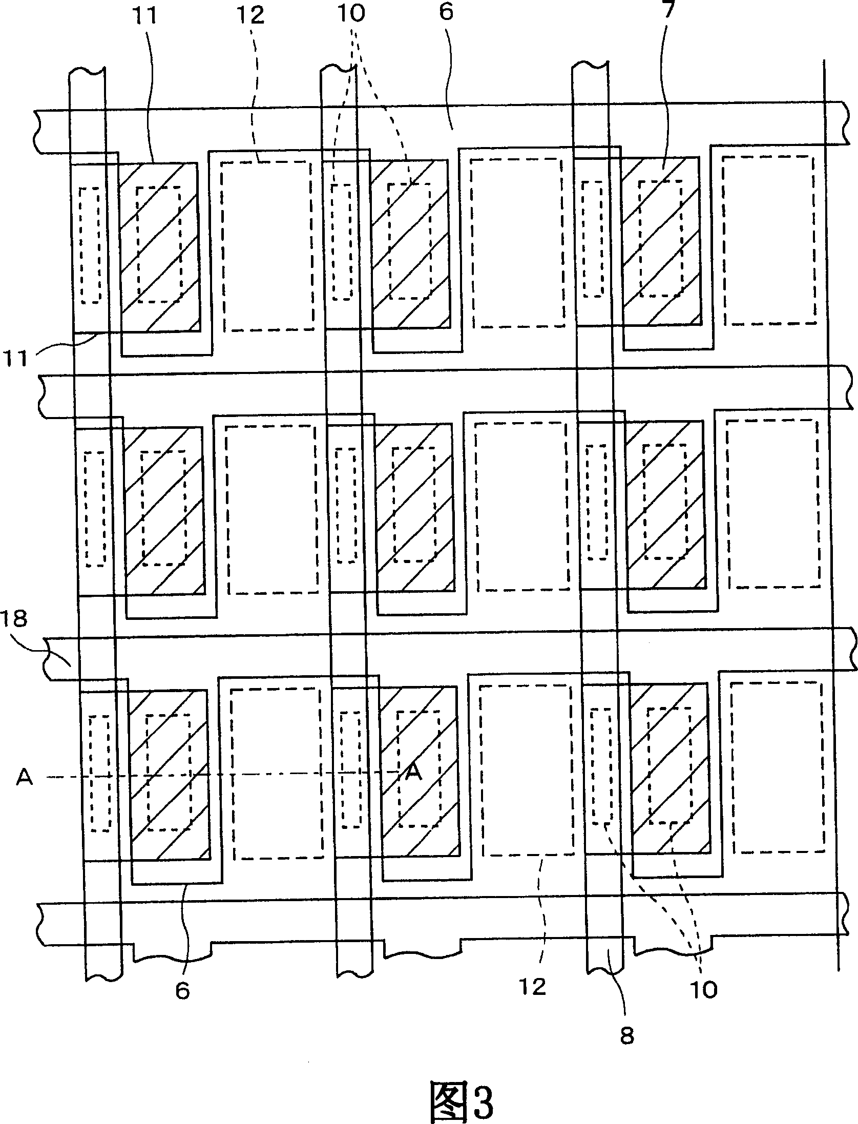
[0023] Hereinafter, embodiments of the present invention will be described in detail with reference to the accompanying drawings. 3 shows a plan view of a unit for detecting fingerprints or veins in the biosensor according to the present embodiment, and FIG. 4 is a longitudinal sectional view along line A-A shown in FIG. 3 .

[0024] As shown in FIG. 4, for example, a louver 2 is placed on a backlight unit 1 composed of LEDs (Light Emitting Diodes). For example, the louver 2 is a louver film having a thickness of about 300 μm, which is composed of a film in which transparent portions and opaque portions are laminated in an alternate manner. A light-receiving substrate is also placed on the louver 2 . In this light-receiving substrate, a sensor element is formed on a transparent insulating substrate 3 composed of, for example, glass. Specifically, an opaque film 4 having an opening 12 is formed on the substrate 3 , a transparent insulating film 5 is formed on the opaque film ...


PUM


Abstract

The present invention relates to a biosensor. The optical biosensor with high efficiency of light reception is capable of reading a fingerprint or a vein pattern. A louver is provided between a backlight unit and a substrate in a sensor for identifying a fingerprint by a process in which light emitted from the backlight unit passes through the substrate and is radiated to a fingerprint that is in contact with the upper surface of a protective layer, and light that is reflected according to the surface irregularity of the fingerprint is received by a semiconductor layer that is a light-receiving element. The emitted light is thereby provided with sharp directivity, and the efficiency of light reception by the sensor is therefore increased.

Description

technical field [0001] The invention relates to an optical biosensor capable of reading fingerprints or vein patterns. Background technique [0002] Biometric authentication through fingerprint or vein pattern recognition has recently been used to secure mobile phones, personal computers and other devices. Fingerprint sensors may operate optically, or operate according to capacitance (for example, see Japanese Laid-Open Patent Application No. 2002-267408), pressure, or other characteristics, and optical sensors and capacitance sensors are advantageous in accurate fingerprint detection. However, capacitive fingerprint sensors have the disadvantage of being susceptible to electrostatic discharge, and since the sensor substrate of an optical fingerprint sensor is a semiconductor, a large sensor is very expensive. In addition, vein print sensors have also been limited to CCD (charge-coupled device) sensors, CMOS (complementary metal-oxide semiconductor) sensors, and other optic...

Claims


Application Information

Patent Timeline
Patent Type & Authority Applications(China)
IPC IPC(8): A61B5/117G06K9/00
CPCG06K9/0004G06K2009/00932G06V40/1318G06V40/14
Inventor 高桥美朝
Owner NEC LCD TECH CORP
Why Eureka
Try Eureka