Method of manufacturing strained-silicon semiconductor device

A technology for conductor components and semiconductors, which is applied in the manufacture of semiconductor/solid-state devices, semiconductor devices, electrical components, etc., and can solve problems such as inconvenience, general products and methods do not have appropriate structures and methods, etc.

Inactive Publication Date: 2007-05-30
TAIWAN SEMICON MFG CO LTD
View PDF0 Cites 2 Cited by
  • Summary
  • Abstract
  • Description
  • Claims
  • Application Information

AI Technical Summary

Problems solved by technology

[0010] It can be seen that the above-mentioned existing semiconductor elements obviously still have inconvenience and defects in product structure, manufacturing method and use, and need to be further improved urgently.
In order to solve the above-mentioned problems, the relevant manufacturers have tried their best to find a solution, but no suitable design has been developed for a long time, and there is no suitable structure and method for general products and methods to solve the above-mentioned problems. This is obviously a problem that relevant industry players are eager to solve

Method used


Image

  • Method of manufacturing strained-silicon semiconductor device
  • Method of manufacturing strained-silicon semiconductor device
  • Method of manufacturing strained-silicon semiconductor device

Examples


Embodiment Construction

[0054] In order to further explain the technical means and effects that the present invention adopts to achieve the intended purpose of the invention, below in conjunction with the accompanying drawings and preferred embodiments, the specific implementation, structure, manufacturing method, Steps, features and effects thereof are described in detail below.

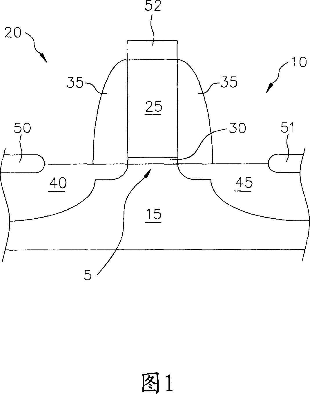
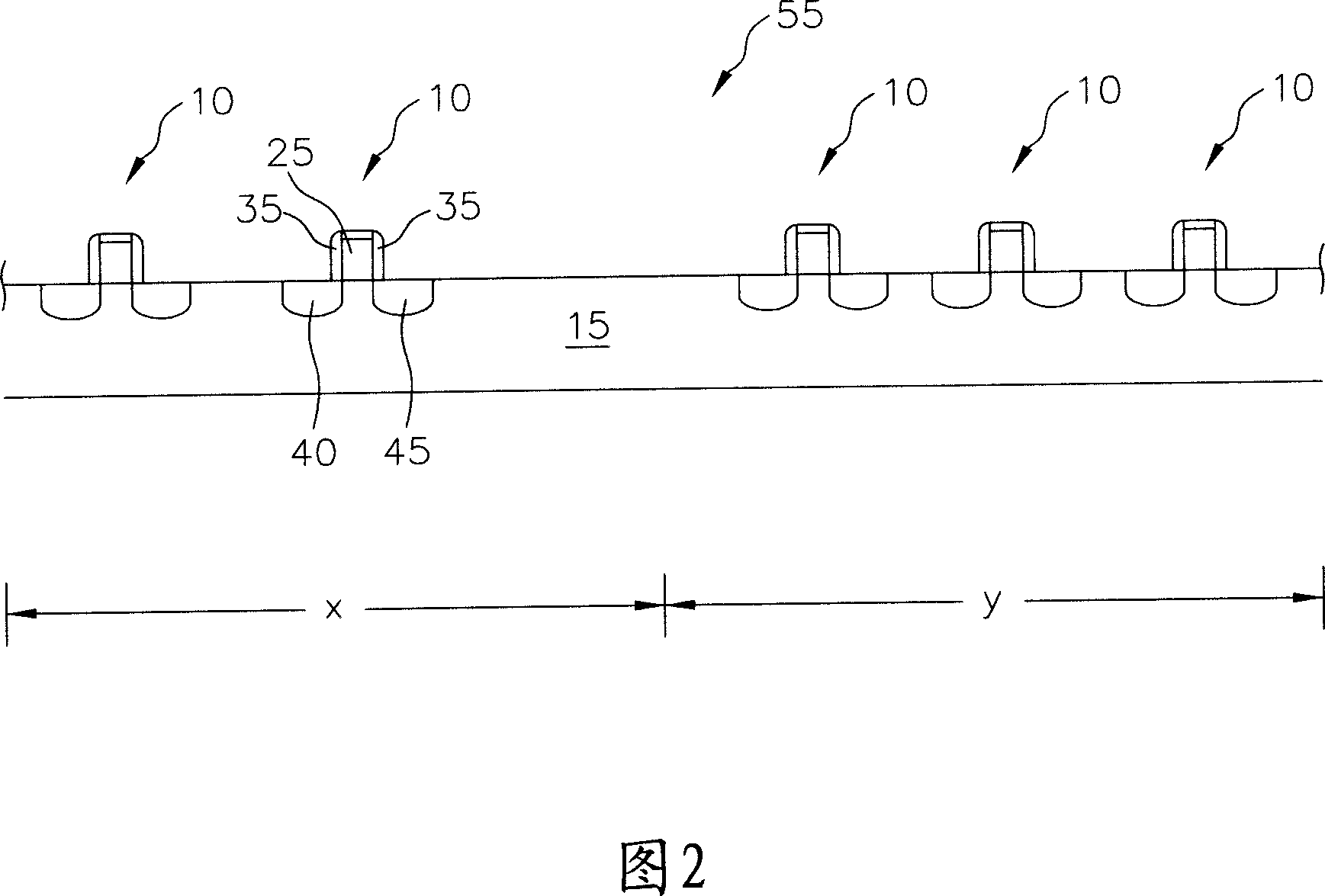
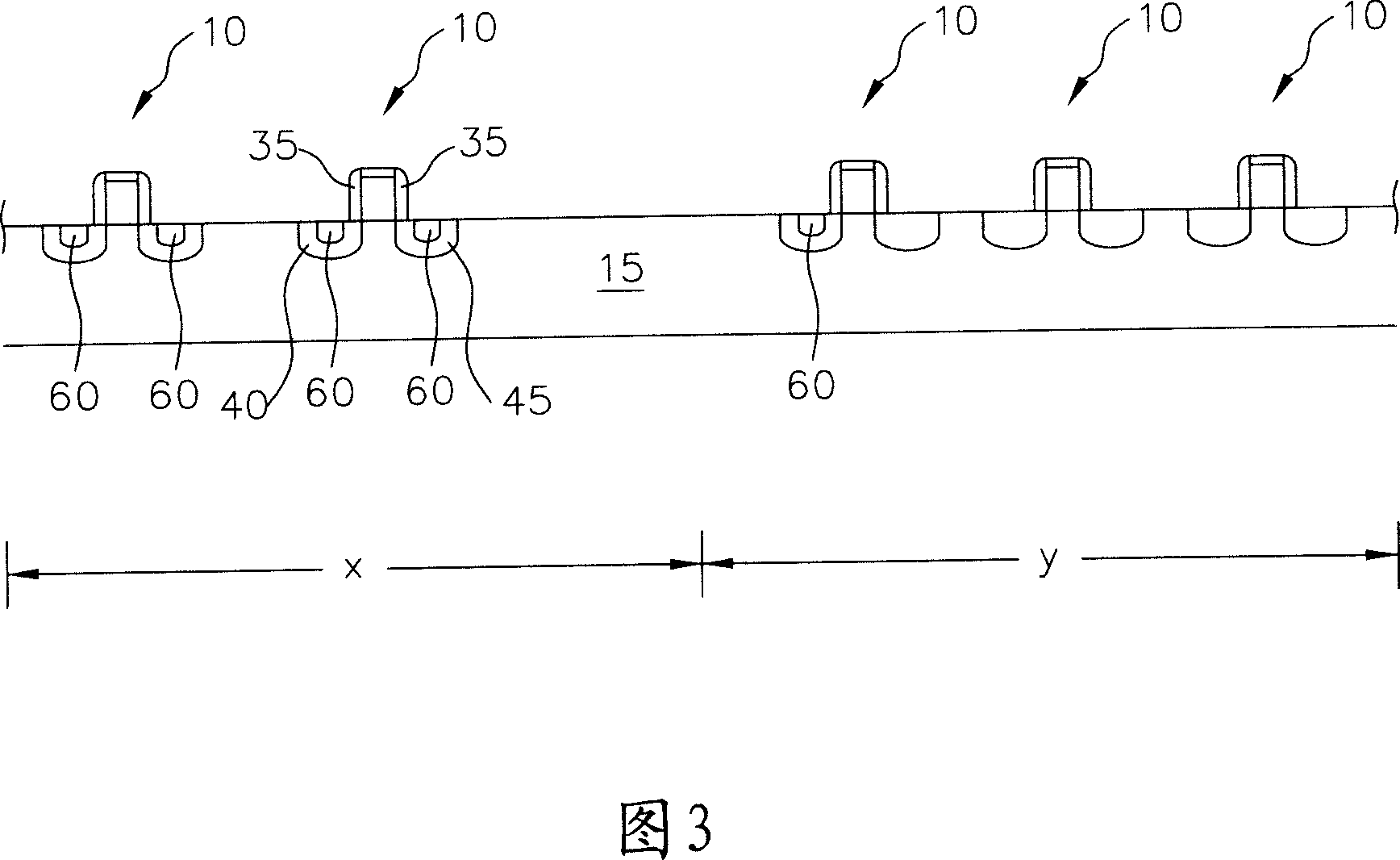
[0055] The making and using of the preferred embodiments of the invention will be described in detail below, however, it will be appreciated that the invention provides many applicable inventive concepts which can be embodied in a wide variety of specific contexts. The embodiments discussed herein are merely illustrative of specific ways to make and use the invention, and do not limit the scope of the invention. The present invention will be described for a preferred embodiment of the specific content, that is, the semiconductor device includes a substrate provided with a plurality of substantially identical transistors. ...


PUM


Abstract

A method for fabricating a strained-silicon semiconductor device to ameliorate undesirable variation in epitaxial film thickness. The layout or component configuration for the proposed semiconductor device is evaluated to determine areas of relatively light or dense population in order to determine whether local-loading-effect defects are likely to occur. If a possibility of such defects occurring exists, a dummy pattern of epitaxial structures may be indicated. If so, the dummy pattern appropriate to the proposed layout is created, incorporated into the mask design, and then implemented on the substrate along with the originally-proposed component configuration. The present invention can decrease or eliminate local load effect without interfering the operation of the semiconductor device.

Description

technical field [0001] The present invention relates to a semiconductor element and its manufacturing method, in particular to a method for manufacturing a semiconductor element to reduce undesired loads when using Selective Epitaxial Growth (SEG) in strained silicon fabrication (Local Loading). Background technique [0002] Electronic devices using semiconductors have been used in a wide variety of applications, providing computing power and data storage and retrieval, enabling not only the operation of large and small computers, but also things such as electronic game consoles, home entertainment systems, telephones and other communication equipment. become possible. Advances in technology have not only enabled the construction of such devices, but have also made them more efficient, more portable, and more affordable. [0003] A semiconductor is actually a material that can form an electrical conductor under certain circumstances, for example: silicon can be treated wit...

Claims


Application Information

Patent Timeline
Patent Type & Authority Applications(China)
IPC IPC(8): H01L21/822H01L21/8232
CPCH01L21/823878H01L27/0207H01L21/823807
Inventor 陈永修章勋明
Owner TAIWAN SEMICON MFG CO LTD
Why Eureka
Try Eureka