Semiconductor device and its manufacturing method

A technology of semiconductors and devices, which is applied in the field of semiconductor devices and their manufacturing, can solve problems such as deterioration of component characteristics and high drain region resistance, and achieve the effects of improving component performance, reducing lead inductance, and reducing power supply noise

Inactive Publication Date: 2007-06-06
SHARP KK
View PDF0 Cites 9 Cited by
  • Summary
  • Abstract
  • Description
  • Claims
  • Application Information

AI Technical Summary

Problems solved by technology

[0005] However, according to the structure of the semiconductor device disclosed in the literature, since the same type of diffusion layer as the drain region is formed so that it can be connected from the front surface through the substrate, the drain region resistance becomes high, which leads to an increase in on-resistance, On-resistance is an important parameter of power devices.
As a result, component characteristics deteriorate

Method used


Image

  • Semiconductor device and its manufacturing method
  • Semiconductor device and its manufacturing method
  • Semiconductor device and its manufacturing method

Examples


no. 1 example

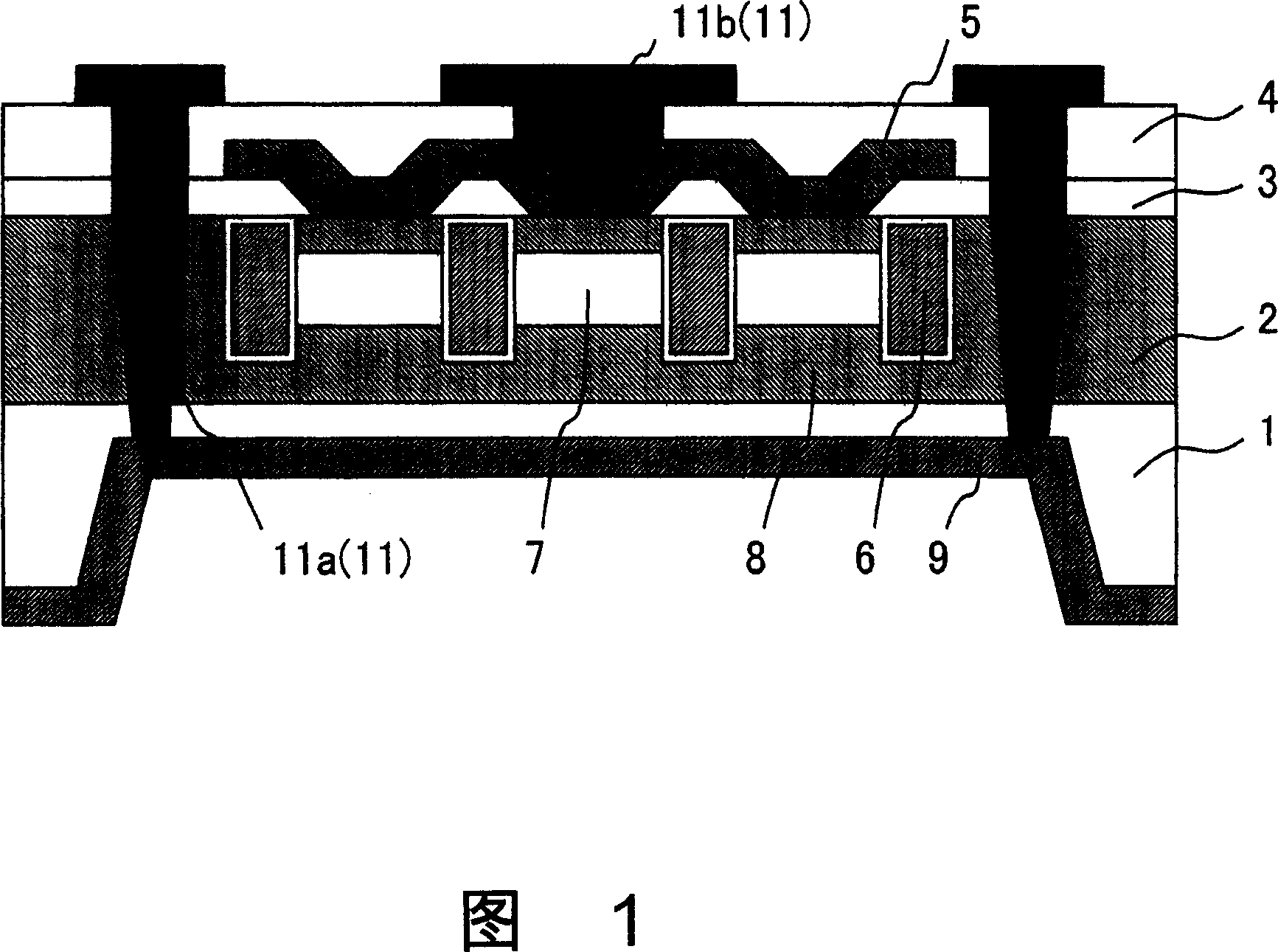
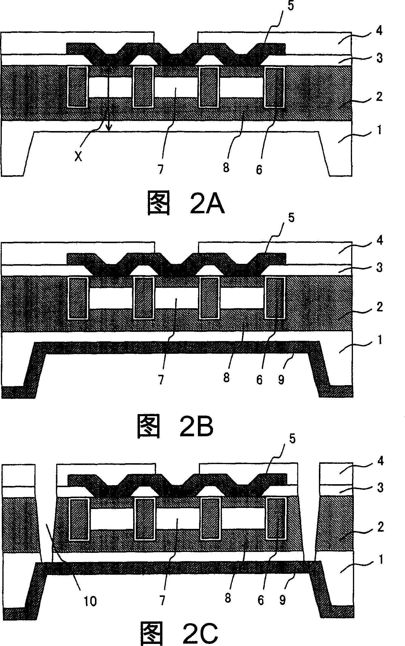
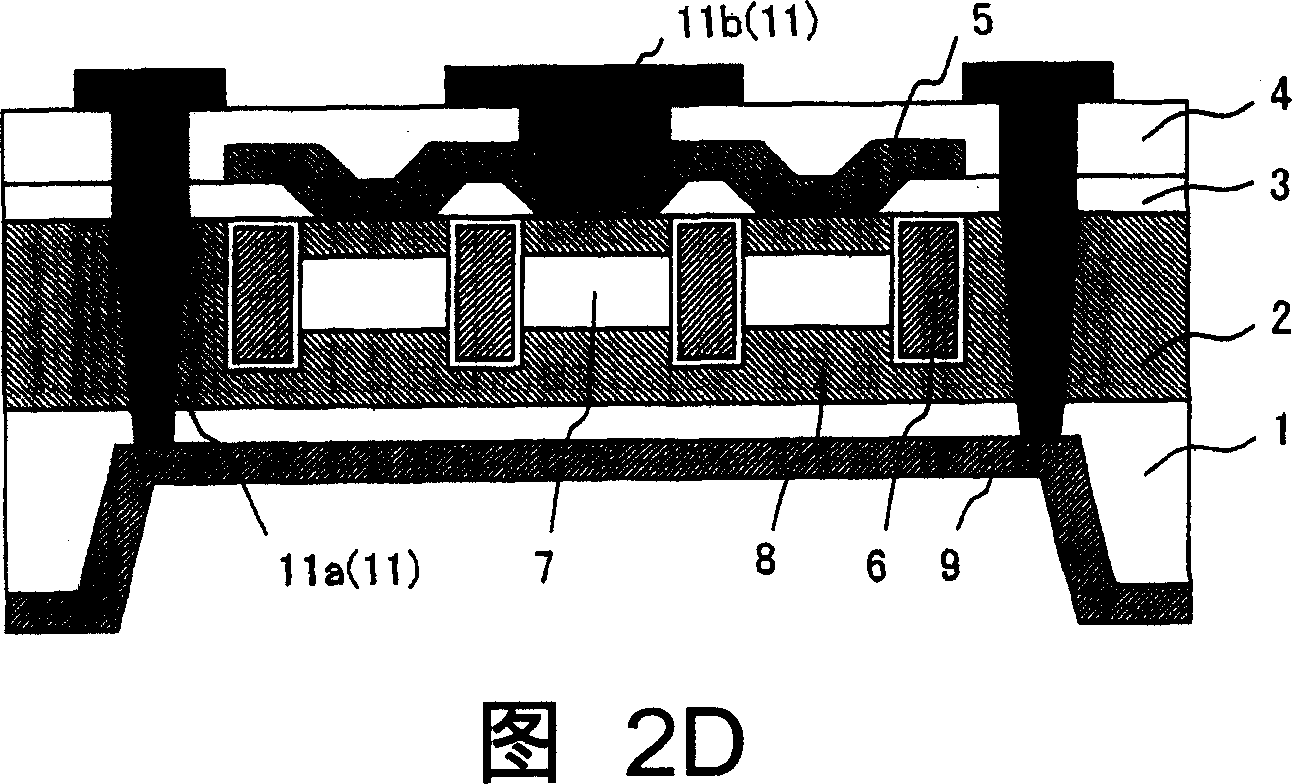
[0023] A device of the present invention and a method of the present invention according to a first embodiment will be described with reference to FIG. 1 and FIGS. 2A to 2D. Here, FIG. 1 is a schematic cross-sectional view showing a schematic configuration of a device of the present invention according to this embodiment.

[0024] The transistor employed in this embodiment is a trench type power MOSFET, and at least one first electrode 11 b provided on the front surface of the silicon substrate 1 is electrically connected to the source electrode of the transistor through a metal lead 5 . Further, through electrode 11 a is electrically connected to the drain electrode of the transistor through a second electrode (metal layer 9 ) provided on the rear surface of silicon substrate 1 . Further, the via electrode 11a is electrically connected to the second electrode (metal layer 9) through a via hole penetrating the semiconductor chip from its front surface to its rear surface. A p...

no. 2 example

[0031] The method of the present invention according to the second embodiment will be described with reference to FIGS. 3A to 3D. In this embodiment, description will be made using a trench type power MOSFET as an example similar to the first embodiment.

[0032] First, a trench type power MOSFET is formed by a conventional process similar to that of the first embodiment. Then, according to this embodiment, as shown in FIG. 3A, the thickness of the silicon substrate 1 is reduced to about 100 [mu]m by grinding the back surface.

[0033]Then, as shown in FIG. 3B, metal layer 9 is formed on the rear surface of silicon substrate 1 by sputtering. In this embodiment, although the material of metal layer 9 is not particularly limited similarly to the first embodiment, a metal material having low resistance is employed to minimize an increase in on-resistance.

[0034] Then, as shown in FIG. 3C, a via hole 10 is formed to reach the metal layer 9 from the front surface of the silicon...


PUM


Abstract

A semiconductor device comprises at least one first electrode (11b) provided on the front surface of a semiconductor chip and electrically connected to at least one of electrodes that constitute a transistor, a second electrode (9) provided on the back surface of the semiconductor chip and electrically connected to one of the other electrodes, a via hole penetrating the semiconductor chip from the front surface to the back surface, and a through electrode (11a) a part of which is exposed on the front surface of the semiconductor chip electrically connected to the second electrode (9) through the via hole.

Description

technical field [0001] The present invention relates to a semiconductor device including at least one first electrode provided on a front surface of a semiconductor chip and electrically connected to at least one of electrodes constituting a transistor, and a method of manufacturing the same, and a semiconductor device provided on a rear surface of the semiconductor chip and electrically connected to a second electrode of one of the other electrodes. More particularly, the present invention relates to flip-chip packaging technology of power semiconductor devices including power MOSFETs. technical background [0002] Power MOSFETs are power devices widely used in various types of power supply circuits and automobiles, etc., and improvements in their performance such as high-speed switching, reduction in on-resistance, etc. are expected. Power MOSFETs mainly include trench type (vertical type) and planar type (lateral type), and trench type power MOSFETs especially have a str...

Claims


Application Information

Patent Timeline
Patent Type & Authority Applications(China)
IPC IPC(8): H01L29/41H01L29/78H01L21/28H01L21/336
CPCH01L2924/13091H01L29/0886H01L29/66734H01L29/7813H01L29/0657H01L29/41741H01L29/7809H01L2924/01078H01L2924/01079H01L23/481H01L2224/16H01L29/41766H01L2924/1305H01L2924/13055H01L2924/00
Inventor 福见公孝A·O·阿丹
Owner SHARP KK
Why Eureka
Try Eureka