Chip resistor and its manufacturing method

A technology for chip resistors and manufacturing methods, applied in the direction of resistors, resistor assemblies, and manufacturing resistor chips, etc., can solve problems such as position deviation, surface electrodes 2 and end surface electrodes 5 cannot be electrically connected, etc.

Inactive Publication Date: 2007-06-27
PANASONIC CORP
View PDF2 Cites 7 Cited by
  • Summary
  • Abstract
  • Description
  • Claims
  • Application Information

AI Technical Summary

Problems solved by technology

However, in such a general method of manufacturing chip resistors, when surface electrodes 2 or resistors 3 are formed by printing, sputtering, etc., positional deviation occurs, and as shown in FIG. Groove 4a, i.e. the opposite side of square substrate 1, in this state, if by dividing sheet-like substrate 1a along primary dividing groove 4a, obtain a plurality of elongated substrates 1b, and as As shown in FIG. 18 , when the end face electrodes 5 are formed on the opposite end faces of the square substrate 1, there will be a problem that the surface electrodes 2 and the end face electrodes 5 cannot be electrically connected.

Method used


Image

  • Chip resistor and its manufacturing method
  • Chip resistor and its manufacturing method
  • Chip resistor and its manufacturing method

Examples


no. 1 example

[0034] Hereinafter, a first embodiment of the present invention will be described.

[0035] FIG. 1 is a plan view of a chip resistor of a first embodiment of the present invention.

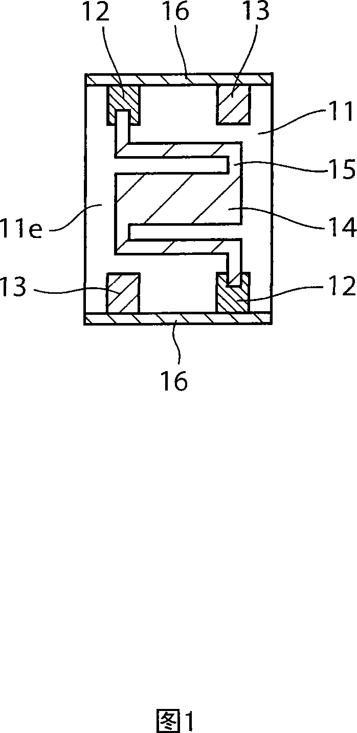
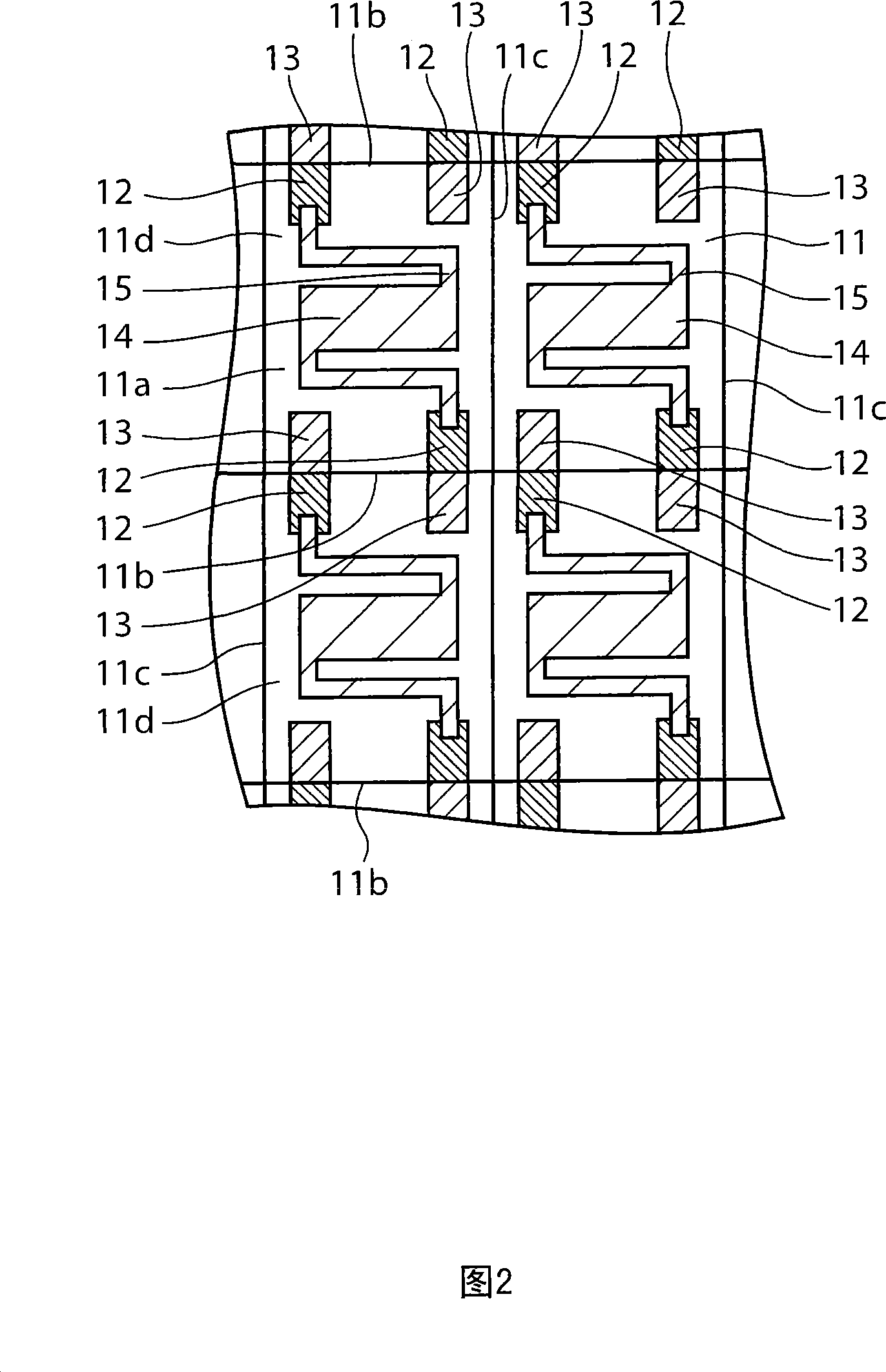
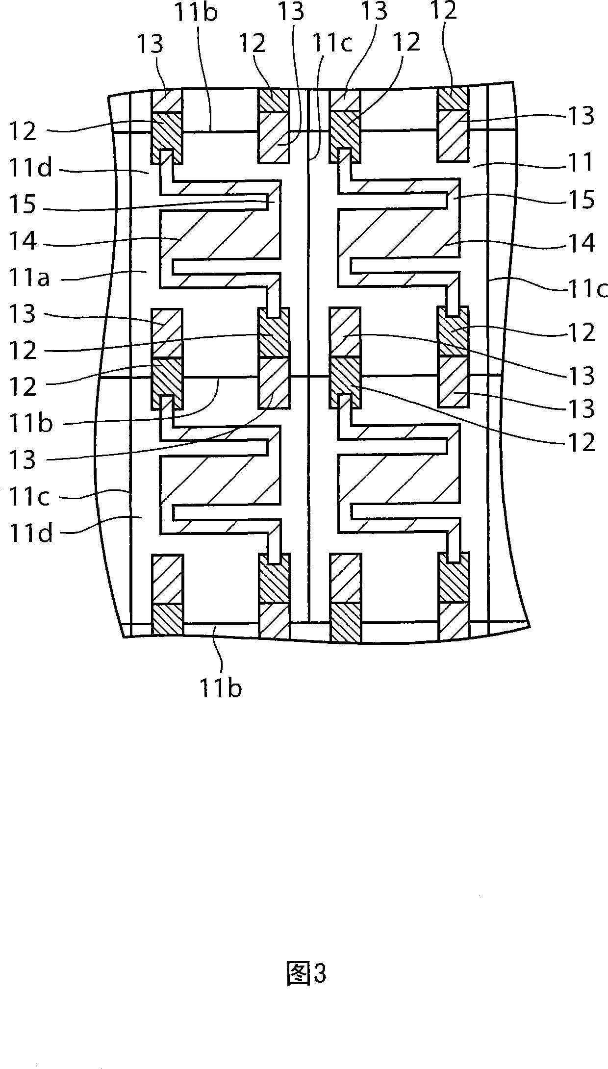
[0036] In FIG. 1, 11 is a square substrate made of alumina, and the planar shape of the square substrate 11 is a rectangle. 12 is two opposite side portions formed on the surface of the above-mentioned square substrate 11, relative to the direction connecting the two opposite side portions of the square substrate 11, that is, the centerline of the longer direction of the square substrate 11 A pair of surface electrodes located on opposite sides, the pair of surface electrodes 12, is formed by screen printing with electrode paste (Electrode Paste) mainly composed of silver and sintering at 850°C. 13 is two opposite sides on the surface of the above-mentioned square substrate 11, relative to the direction perpendicular to the direction connecting the opposite two sides of the above-mentioned square...

no. 2 example

[0053] Next, a second embodiment of the present invention will be described.

[0054] 7 is a plan view of a chip resistor of a second embodiment of the present invention.

[0055]In FIG. 7, 21 is a square substrate made of alumina, and the planar shape of the square substrate 21 is a rectangle. 22 is two opposite side portions formed on the surface of the above-mentioned square substrate 21, relative to the direction connecting the two opposite side portions of the square substrate 21, that is, the center line in the longer direction of the square substrate 21. A pair of surface electrodes located on the opposite side, the pair of surface electrodes 22, is formed by screen printing with an electrode paste mainly composed of silver, followed by sintering at 850°C. 23 is two opposite sides on the surface of the above-mentioned square substrate 21, relative to the direction connecting the opposite two sides of the above-mentioned square substrate 21, that is, the direction perpe...

no. 3 example

[0074] Next, a third embodiment of the present invention will be described.

[0075] 13 is a plan view of a chip resistor of a third embodiment of the present invention.

[0076] In FIG. 13, 31 is a square substrate made of alumina, and the planar shape of the square substrate 31 is a rectangle. 32 is a pair of surface electrodes formed on two opposite sides of the surface of the above-mentioned square substrate 31 along the extending direction of the two sides, that is, the shorter direction of the square substrate 31, the pair of surface electrodes 32. It is made by screen printing with silver-based electrode paste and sintered at 850°C. 34 is a resistor body formed on the surface of the square substrate 31, spanning between the above-mentioned pair of surface electrodes 32, and electrically connected thereto. Screen printing and sintering at 850°C. The above-mentioned resistor 34 has a meandering portion 35 meandering across between a part of the pair of surface electrodes...


PUM


Abstract

A chip resistor comprises a pair of upper-face electrodes formed on two confronting side portions of a square substrate such that they are positioned on the sides opposed to each other with respect to the center line of the square substrate extending in the direction joining the two side portions, a resistor formed on the square substrate such that it is electrically connected with the paired upper-face electrodes, and a pair of end-face electrodes formed on the end faces of the two confronting side portions of the square substrate and electrically connected with the paired upper-face electrodes. The chip resistor further comprises dummy electrodes formed individually at the two confronting side portions of the square substrate such that they are positioned to correspond to the paired upper-face electrodes in the direction joining the two side portions.

Description

technical field [0001] The present invention relates to a chip resistor used in various electronic devices and a manufacturing method thereof. Background technique [0002] In the conventional chip resistor (Chip Resistor), in order to improve load characteristics such as pulse resistance characteristics by enlarging the area of ​​the resistor body and lengthening the length of the resistor body, as shown in FIG. Between the opposite sides of the square substrate 1, a pair of surface electrodes 2 are formed so that one of them and the other are on opposite sides to each other with respect to the centerline of the square substrate 1 in the direction connecting the opposite sides. , and then, a circuitous resistor body 3 electrically connected to the pair of surface electrodes 2 is formed. [0003] In the above-mentioned conventional chip resistors, since the width of a pair of surface electrodes 2 is made to be less than half of the length of the opposing sides, when forming...

Claims


Application Information

Patent Timeline
Patent Type & Authority Applications(China)
IPC IPC(8): H01C7/00H01C17/06
CPCY10T29/49082H01C17/28H01C1/14H01C17/006H01C7/001
Inventor 井关健有贺秀二中尾光明
Owner PANASONIC CORP
Why Eureka
Try Eureka