Display device

A display device and surface configuration technology, which can be applied to static indicators, cathode ray tube indicators, instruments, etc., and can solve the problems that the display device cannot be embedded in the wall

Active Publication Date: 2007-07-04
AU OPTRONICS CORP
0 Cites 10 Cited by

AI-Extracted Technical Summary

Problems solved by technology

For example, the distance from the light source cannot be too far, or although LCD TVs are becoming thinner and thinner, and the market demand for wall-mounting is emphasized, t...

Method used

[0034] In the display device disclosed in the above-mentioned embodiments of the present invention, the light guide element is designed through the irregular structure of the second surface and the proportional relationship between the diameter of the inscribed circle and the relative distance between the first surface and the second surface, so that the light The sensor detects sufficient brightness and improves the light loss problem caused by traditional light pipes when light enters at a large incident angle. Thus, the flex...

Abstract

The invention discloses a display device that comprises a casing, a screen, a photoconductive cell, a photoreceptor and a control circuit. The screen is set on front of the casing. The photoconductive cell is used to guide a beam, and the photoconductive cell includes a first surface, a second surface and a side surface. The first surface is used to receive light beam, and the first surface is on front of the casing; the second surface is used to lead out the beam, the second surface possesses a irregular structure to decrease the total reflection light flux; the side surface connects the edge of the first surface and the second surface, and the light flux that beam is refracted from the first surface to the second surface is bigger than the light flux that beam is refracted from the first surface to the side surface. The photoreceptor is mounted in the casing and faced to the second surface, it is used to receive the beam lead out from the second surface and output a signal. The control circuit is couple connected with the screen and the photoreceptor, and adjust the brightness of the screen according to signal.

Application Domain

Cathode-ray tube indicators

Technology Topic

PhotodetectorLight flux +5

Image

  • Display device
  • Display device
  • Display device

Examples

  • Experimental program(1)

Example Embodiment

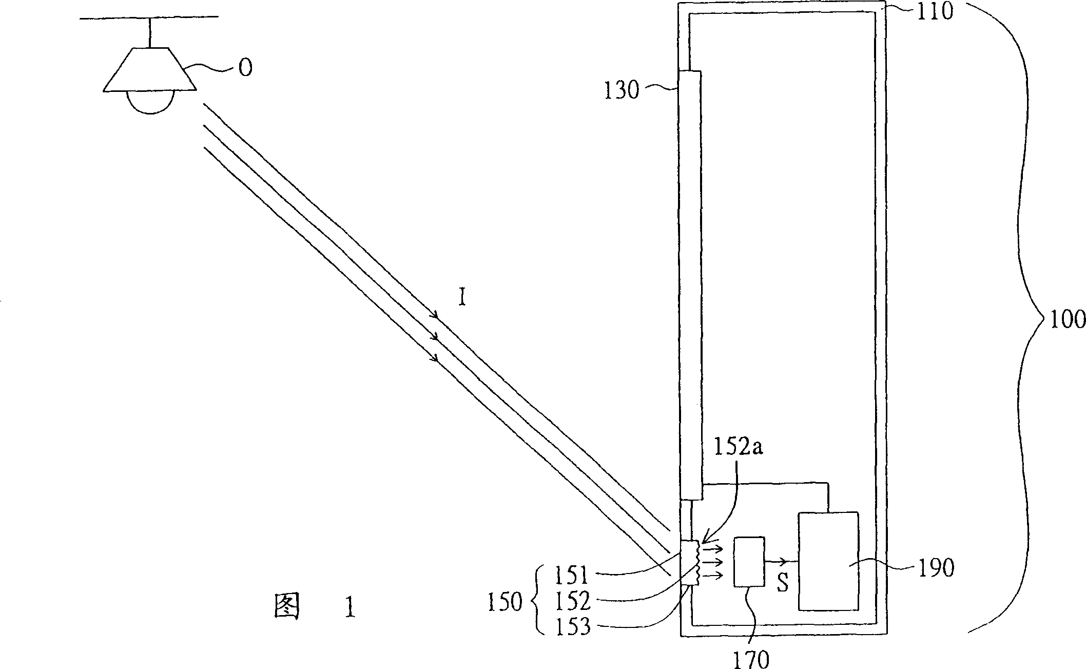
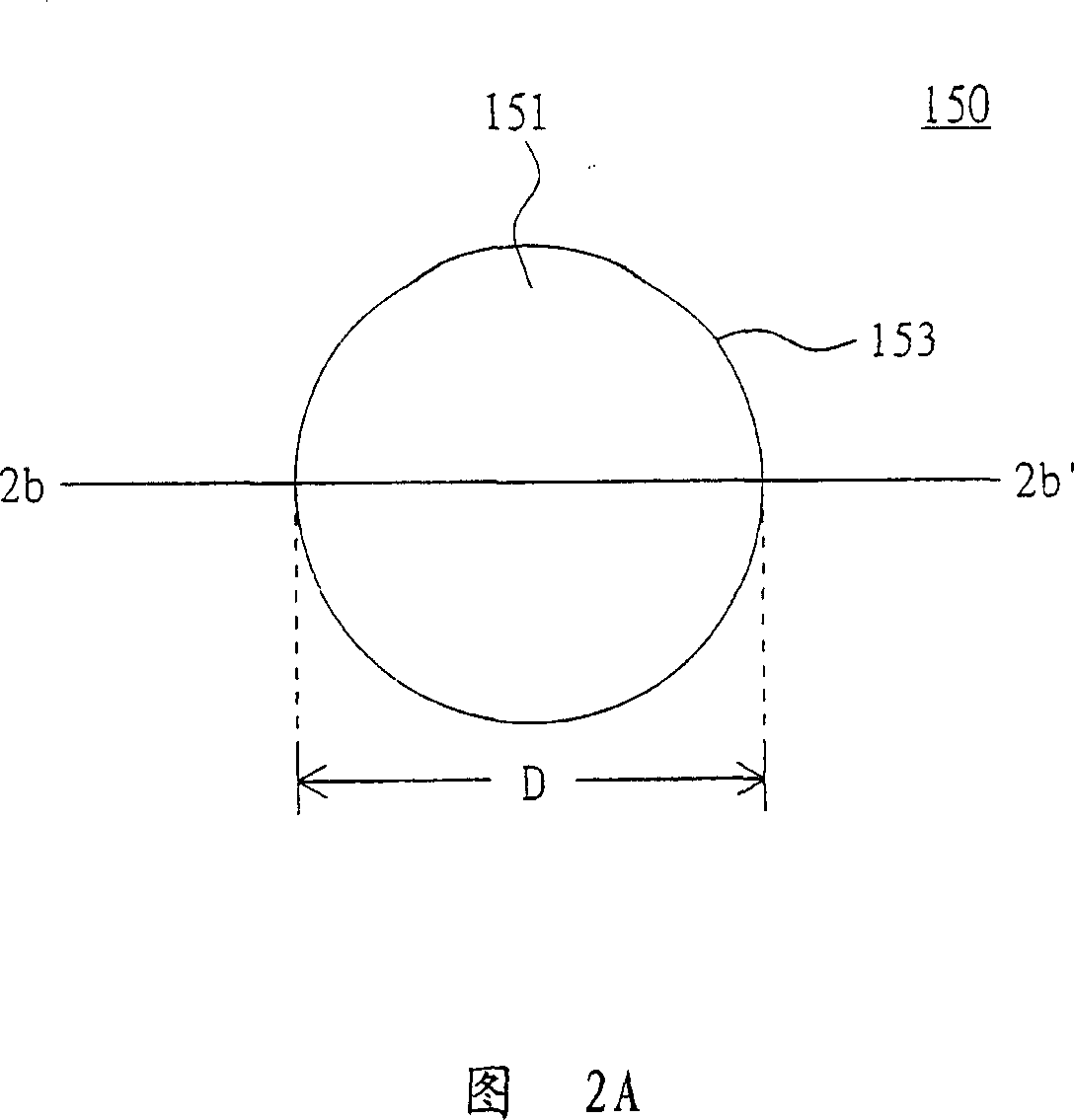
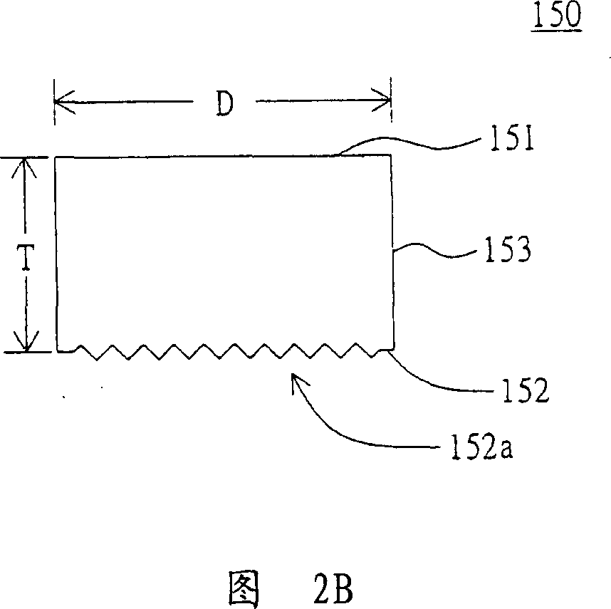
[0027] Please refer to FIG. 1 , which is a schematic diagram illustrating that the display device according to the preferred embodiment of the present invention adjusts the screen brightness according to the ambient brightness. The display device 100 is, for example, a liquid crystal television or a plasma television, and includes a casing 110 , a screen 130 , a light guide element 150 , a light sensor 170 and a control circuit 190 . The screen 130 is disposed on the front of the casing 110 . The light guide element 150 is, for example, a transparent material, such as Poly Methyl Methacrylate (PMMA), MS resin, Poly Carbonate (PC), and Polyethylene terephthalate (Polyethylene terephthalate). Terephthalate, PET) and so on. The light guide element 150 is used to receive and guide a light beam I emitted by the light source O, and the light guide element 150 includes a first surface 151 , a second surface 152 and a side surface 153 .
[0028] The first surface 151 is used for receiving the light beam I, and the first surface 151 is disposed on the front surface of the casing 110 . The second surface 152 is used for deriving the light beam I, and relative to the first surface 151, the second surface 152 has an irregular structure 152a for reducing the total reflected light flux of the light beam I on the second surface 152; the irregular structure 152a is, for example, A bite flower structure (texture). The side surface 153 connects the edges of the first surface 151 and the second surface 152 , and the luminous flux of the light beam I refracted to the second surface 152 through the first surface 151 is greater than the luminous flux of the light beam I refracted to the side surface 153 through the first surface 151 . The light sensor 170 is, for example, a Charge Coupled Device (CCD), a Complementary Metal-Oxide Semiconductor (CMOS), or any light sensor capable of sensing the brightness of light; light sensing The device 170 is disposed in the casing 110 and faces the second surface 152 for receiving the light beam I derived from the second surface 152 and outputting a signal S accordingly. The control circuit 190 is coupled to the screen 130 and the light sensor 150 and adjusts the brightness of the screen 130 according to the signal S.
[0029] In addition, the light guide element 150 is substantially a cylinder, the first surface 151 and the second surface 152 are substantially the same shape, and the first surface 151 is a circle or a polygon. In this embodiment, the first surface 151 is described by taking a circle as an example. As for how the light guide element 150 restricts the luminous flux of the light beam I refracted to the second surface 152 through the first surface 151 to be greater than the luminous flux of the light beam I refracted to the side surface 153 through the first surface 151 in a proportional relationship in size, and how it guides The light beam I is directed to the photo sensor 170, which is described in this figure as follows, but the technology of the present invention is not limited thereto.
[0030] Please refer to FIGS. 2A-2B. FIG. 2A is a top view of the structure of a light guide element according to a preferred embodiment of the present invention, and FIG. 2B is a view along the section line 2b-2b' of FIG. 2A. A cross-sectional view of the structure of the light guide element. 2A omits the drawings and labels of the second surface 152, and the section line 2b-2b' passes through the center of the first surface 151. According to the present invention, a diameter D of an inscribed circle of the first surface 151 is substantially greater than N times a relative distance T between the first surface 151 and the second surface 152 , wherein N is greater than 1. When the first surface 151 is circular, as shown in FIG. 2A , the diameter D of the inscribed circle is the diameter of the first surface 151 . In this embodiment, N is preferably 1.72.
[0031] With the limitation of N, after the light beam I enters the light guide element 150 through the first surface 151 , the light flux directly incident on the second surface 152 can be increased compared with the conventional light guide pipe. That is, even if the light beam I has a larger incident angle, such as greater than 42 degrees, after entering the light guide element 150 from the first surface 151, compared with the traditional light guide pipe, the light flux incident to the side surface 153 can be reduced, and further The loss of light quantity refracted out of the light guide element 150 through the side surface 153 is reduced. In addition, when the light beam I enters the light guide element 150 via the first surface 151 at a relatively large incident angle, the incident angle to the second surface 152 may reach the critical angle of total reflection when it hits the second surface 152 . At this time, the irregular structure 152a of the second surface 152 is used to change the detail angles of the second surface 152, so that the luminous flux of the light beam I refracted out of the second surface 152 is increased to achieve the desired light guiding effect.
[0032] Please refer to FIG. 3 , which is a schematic diagram of a light guide element leading out a light beam according to a preferred embodiment of the present invention. For example, the light guide element 150 is made of ordinary glass, the diameter D of the first surface 151 is 5.5 unit length, and the relative distance T between the first surface 151 and the second surface 152 is 3.17 unit length. At this time, even if the light beam I enters the light guide element 150 through the first surface 151 at an incident angle of 89 degrees, and exits through the second surface 152, the deriving luminous flux still has the luminous flux when the light beam I enters the first surface 151 more than 50%. In this way, the light sensor 170 receives enough brightness to correctly output the signal S, and the control circuit 190 appropriately adjusts the brightness of the screen 130 according to the signal S.
[0033] Although the display device 100 of this embodiment is described by taking an LCD TV or a plasma TV as an example, the light guide element 150 of this embodiment can also be applied to various display devices that must perform feedback control of internal circuits according to external brightness. In addition, those with ordinary knowledge in the technical field to which the present invention pertains can also understand that when the light guide element 150 is made of various polygons such as regular polygons or materials with different refractive indices, the proportional relationship between the diameter D of the inscribed circle and the relative distance T can also be used. Adjust the overall size of the light guide element 150 to achieve the desired light guide effect.
[0034] In the display device disclosed in the above-mentioned embodiments of the present invention, the light guide element of the light guide element is designed through the irregular structure of the second surface and the proportional relationship between the diameter of the inscribed circle and the relative distance between the first surface and the second surface, so that the light sensor is It can sense enough brightness and improve the problem of light loss caused by the traditional light guide when the light enters at a large incident angle. Therefore, the flexibility of the placement position of the light guide element on the casing of the display device is increased, and at the same time, the placement position of the display device is greatly facilitated. Furthermore, the overall size of the light guide element can be adjusted as required, for example, the relative distance between the first surface and the second surface can be shortened, so as to meet the increasingly thin and light market demands of display devices.
[0035]To sum up, although the present invention is disclosed in conjunction with the above preferred embodiment, it is not intended to limit the present invention. Anyone familiar with this technology can make various modifications without departing from the spirit and scope of the present invention. Therefore, the protection scope of the present invention should be defined by the claims.

PUM

no PUM

Description & Claims & Application Information

We can also present the details of the Description, Claims and Application information to help users get a comprehensive understanding of the technical details of the patent, such as background art, summary of invention, brief description of drawings, description of embodiments, and other original content. On the other hand, users can also determine the specific scope of protection of the technology through the list of claims; as well as understand the changes in the life cycle of the technology with the presentation of the patent timeline. Login to view more.
Why Eureka
Try Eureka