Unlock instant, AI-driven research and patent intelligence for your innovation.

Substrate checking device and method

A substrate inspection and substrate technology, applied in the direction of measuring devices, electronic circuit testing, instruments, etc., can solve problems such as difficult to use, difficult four-terminal measurement, unable to configure probes, etc., to achieve simplified wiring, effective four-terminal measurement, simple four-terminal Effect of terminal measurement

Inactive Publication Date: 2007-07-11
NIDEC-READ CORPORATION
View PDF1 Cites 27 Cited by
  • Summary
  • Abstract
  • Description
  • Claims
  • Application Information

AI Technical Summary

Problems solved by technology

[0006] The four-terminal probe disclosed in this publication can be used on the side of the ball grid surface of a wiring pattern formed with a wide wiring pitch, but it is not suitable for a wire pattern formed with a narrow wiring pitch. It will be difficult to use on the flip chip package (flip chip) surface with high-density wiring pattern
[0007] This is because the number of four-terminal probes per unit area increases when the four-terminal probes are brought into contact with the inspection surface side of the substrate on which a high-density wiring pattern with a narrow wiring pitch is formed like the flip-chip package surface. , resulting in the inability to configure the necessary number of probes
[0008] Furthermore, the four-terminal probe disclosed in the above-mentioned publication has the following problem, that is, it is difficult to perform four-terminal measurement on a substrate where the following two types of wiring are present at the same time

Method used


Image

  • Substrate checking device and method
  • Substrate checking device and method
  • Substrate checking device and method

Examples


Embodiment Construction

[0039] Hereinafter, embodiments of the present invention will be described with reference to the drawings.

[0040] [Four-terminal measuring device]

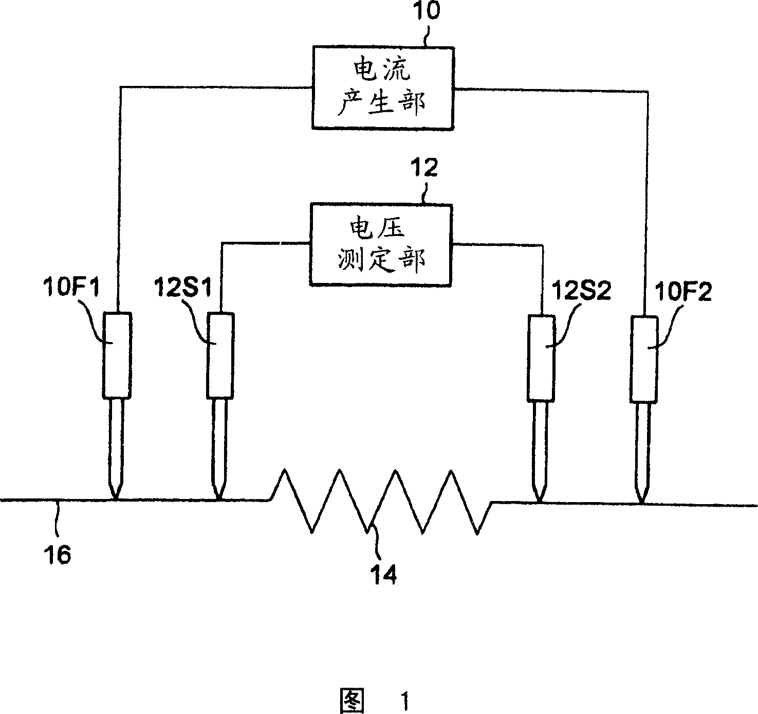
[0041] FIG. 1 is an explanatory diagram for explaining the concept of a four-probe measurement method. This device includes a current generating unit 10 and a voltage measuring unit 12 . The first and second current probes 10F1 and 10F2 for current supply are connected to the current generator 10 , and the first and second voltage probes 12S1 and 12S2 for voltage measurement are connected to the voltage measurement unit 12 .

[0042] As shown in FIG. 1, when measuring the resistance 14 of the wiring of the circuit board 16, the first and second voltage probes 12S1, 12S2 and the first voltage probes 12S1 and 12S2 are arranged in contact with both ends of the wiring whose resistance 14 should be measured. and the second current probes 10F1, 10F2, and a current of a predetermined magnitude for measuring the resistance 14 of the w...


PUM


Abstract

The present invention provides substrate inspection device capable operating four terminals measurement to a high density wiring pattern. The substrate inspection device uses a plurality of probes for inspection, the probes for inspection contact with a substrate to be inspected which is arranged to have a plurality of inspection points and has a plurality of wirings. Each probe for inspection is composed of probe for voltage measurement and probe for current supply. The substrate inspection device also has a connection member connecting probes for current supply each other by set; a current supply unit supplying current to the set by the connection member; a voltage measuring unit for measuring voltage between probe for voltage measurement corresponding to the probe for current supply belonging to the set and probe for voltage measurement corresponding to the probe for current supply not belonging to the set but the others; a calculating unit for calculating resistance value of wiring between above two points to be inspected.

Description

technical field [0001] The present invention relates to a substrate inspection device and a substrate inspection method. More specifically, the present invention relates to a substrate inspection device and method for measuring the resistance value of wiring on a circuit board or inspecting for disconnection using a four-terminal measurement method. [0002] The term "circuit substrate" used in this specification and claims is not limited to packaging substrates or film carriers for semiconductor packaging, but printed wiring substrates, flexible substrates, multilayer wiring substrates, liquid crystal substrates, etc. Generic term for various wiring boards such as electrode plates for displays and plasma displays. That is, the term "circuit board" includes all boards that can be measured with four terminals. Background technique [0003] Conventionally, for example, in the conduction inspection of the wiring of a semiconductor package substrate, probes are brought into con...

Claims


Application Information

Patent Timeline
Patent Type & Authority Applications(China)
IPC IPC(8): G01R27/04G01R27/14G01R31/00G01R31/28G01R31/02G01R1/073H05K3/00
Inventor 戒田理夫
Owner NIDEC-READ CORPORATION