Touch panel having sensing structures in visible and non-visible areas and fabrication method thereof

a technology of sensing structure and touch panel, which is applied in the field of touch panel, can solve the problems short circuit and electric short circuit, and achieve the effects of reducing the fabrication yield of the touch panel, preventing the effect of effective etching of the sensing structure, and improving the fabrication yield rate of the touch panel

Active Publication Date: 2018-07-24
TPK TOUCH SOLUTIONS (XIAMEN) INC
View PDF4 Cites 0 Cited by
  • Summary
  • Abstract
  • Description
  • Claims
  • Application Information

AI Technical Summary

Benefits of technology

[0009]A rise on the surface feature at the changing position (e.g. the boundary portion described above) may reduce the fabrication yield of the touch panel may. For example, in the procedure of forming a patterned sensing structure (including a first sensing structure and a second sensing structure), a problem of accumulation of resists may exist at the boundary portion of the visible area and the non-visible area, thereby blocking the sensing structure from being etched effectively. As a result, by designing the adjacent sensing electrodes (including a first sensing electrode and a second sensing electrode) at the boundary portion to have a larger pitch therebetween than those at the other positions, the electrical short circuit resulting from the imperfection in the etching of the sensing structure among the sensing electrodes can be prevented, thereby improving the fabrication yield rate of the touch panels.

Problems solved by technology

In the procedure of the patterning process, the rise on the surface feature may cause the accumulation of resists, which may block the unpatterned sensing electrodes from being etched effectively, creating an electrical short circuit among the sensing electrodes, and reducing the fabrication yield of the touch panels.

Method used


Image

  • Touch panel having sensing structures in visible and non-visible areas and fabrication method thereof
  • Touch panel having sensing structures in visible and non-visible areas and fabrication method thereof
  • Touch panel having sensing structures in visible and non-visible areas and fabrication method thereof

Examples


Embodiment Construction

[0022]The following embodiments are disclosed with accompanying diagrams for detailed description. For illustration clarity, many details of practice are explained in the following descriptions. However, it should be understood that these details of practice do not intend to limit the present disclosure. That is, these details of practice are not necessary in parts of embodiments of the present disclosure. Furthermore, for simplifying the drawings, some of the conventional structures and elements are shown with schematic illustrations.

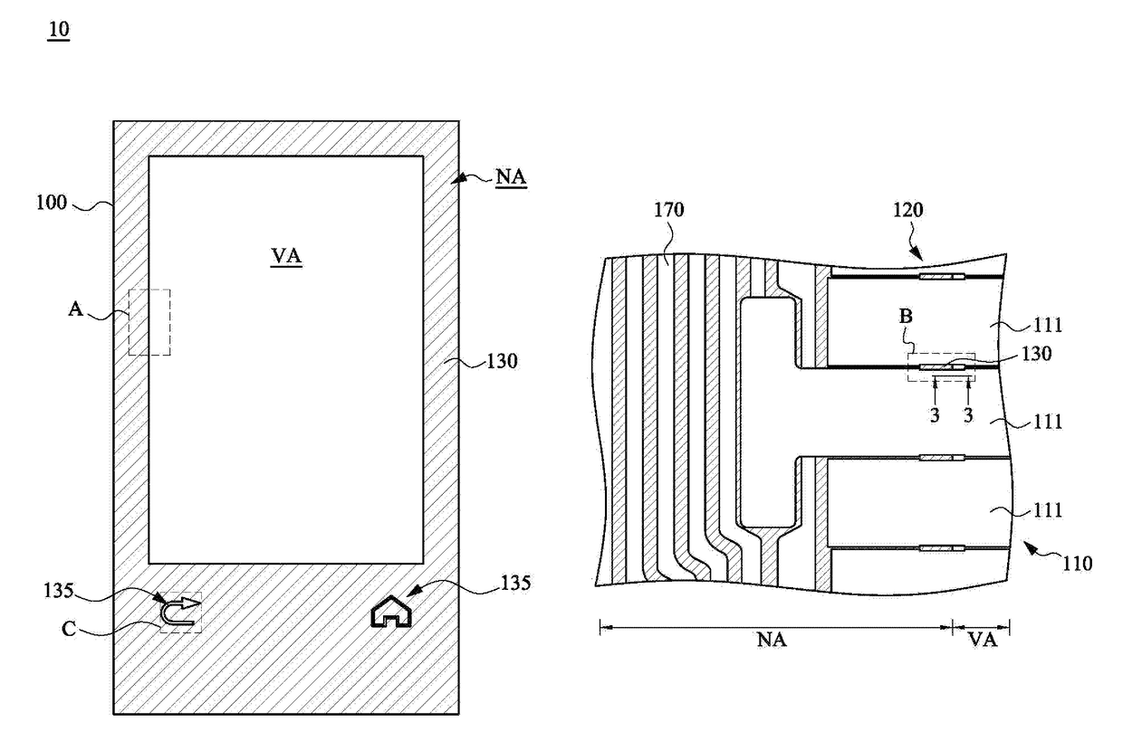
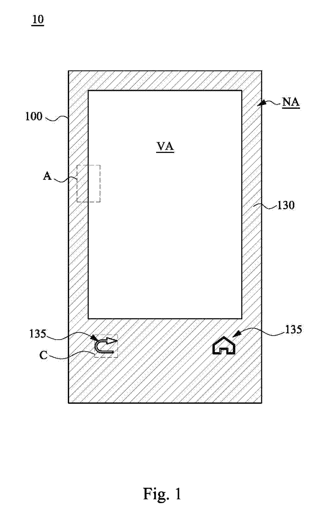
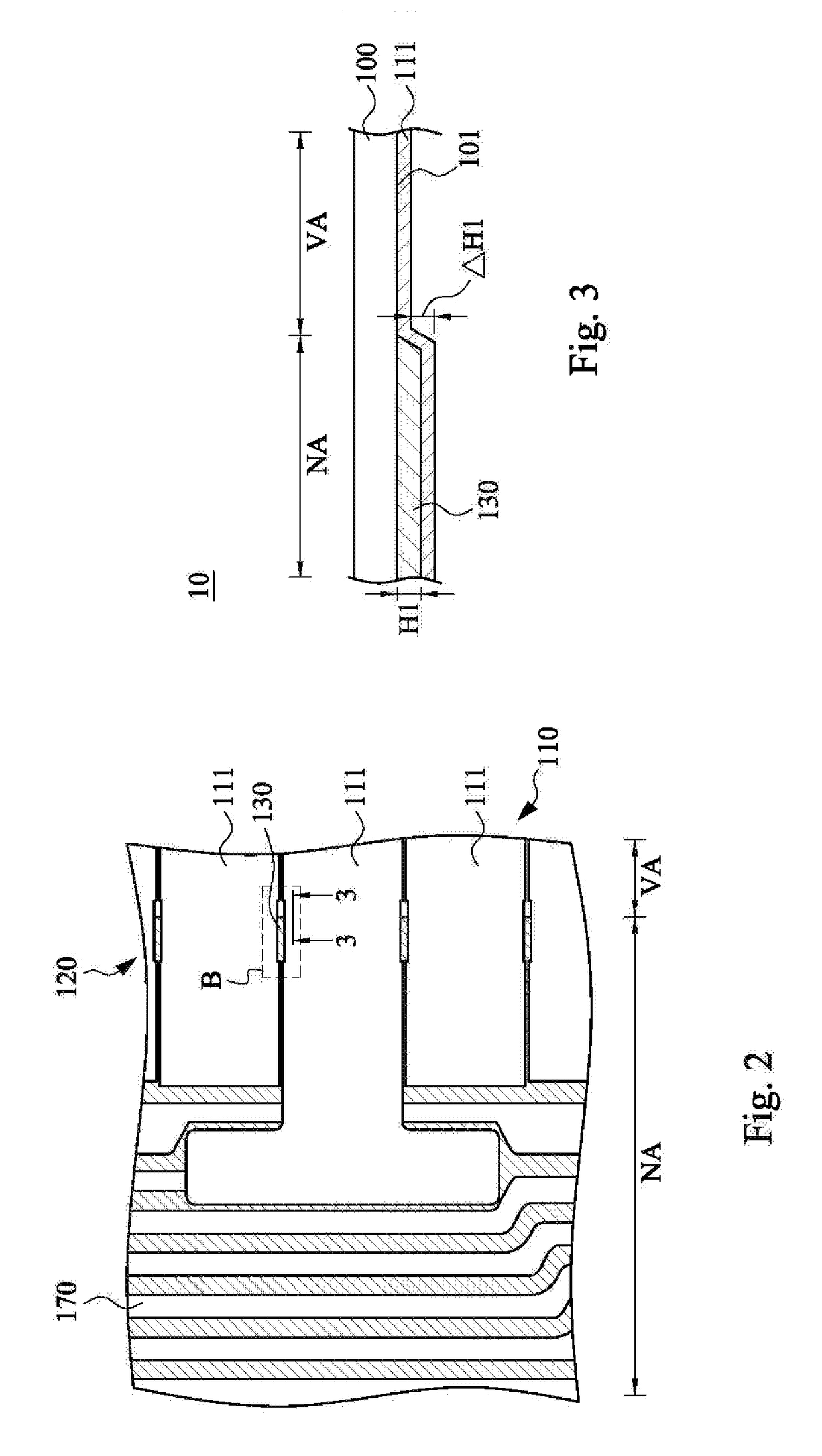
[0023]FIG. 1 is a top view of a touch panel 10 according to an embodiment of the present disclosure. As shown in FIG. 1, the touch panel 10 includes a cover plate 100. The cover plate 100 has a visible area VA and a non-visible area NA. In the embodiment of FIG. 1, the non-visible area NA is disposed at the four sides of the visible area VA, and the non-visible area NA surrounds the visible area VA. To be specific, the touch panel 10 may include a shie...


PUM

PropertyMeasurementUnit
heightaaaaaaaaaa
conductiveaaaaaaaaaa
distanceaaaaaaaaaa

Abstract

A micro-light emitting diode (micro-LED) display device includes a substrate and a micro-LED. The substrate has at least one first metal layer. The micro-LED includes a light emitting structure, at least one second metal layer, at least one reflective layer, and a dielectric layer with an opening. The second metal layer forms a eutectic system or soldering contact with the first metal layer. The reflective layer is disposed between the light emitting structure and the second metal layer, and a eutectic point of the eutectic system or soldering point is lower than a melting point of the reflective layer. The dielectric layer is disposed between the light emitting structure and the reflective layer

Description

BACKGROUND OF THE INVENTION[0001]This application claims priority to Chinese Application Serial Number 201510116749.7, filed Mar. 18, 2015, which is herein incorporated by reference.FIELD OF INVENTION[0002]The present disclosure relates to a touch technology. More particularly, the present disclosure relates to a touch panel and a fabrication method thereof.DESCRIPTION OF RELATED ART[0003]In the present market of various consumer products, touch panels have been widely applied in portable electronic products, such as smartwatches, smartphones, tablet personal computers, notebook personal computers, etc., as the human machine interface (HMI). In addition, since the present electronic products are designed to be light, thin, short, and small, the space accommodating the input device (e.g. button) on the product has become smaller and smaller. As a result, with the trend of perusing user-friendly design of the tablet personal computers, touch panels have become one of the critical comp...

Claims


Application Information

Patent Timeline
Patent Type & Authority Patents(United States)
IPC IPC(8): G06F3/041
CPCG06F3/041G06F2203/04103
Inventor LIN, YANCHIU, TSUNG-KESU, YUNCONGZHANG, ZHUANYUANLIN, YALU
Owner TPK TOUCH SOLUTIONS (XIAMEN) INC
Why Eureka
Try Eureka