Optical module

a technology of optical modules and optical elements, applied in the field of optical modules, can solve the problems of laser output or cost, laser output or constraints, and the wiring cannot be routed to the terminals located inside the full grid, and achieve the effect of improving the reflection characteristi

Active Publication Date: 2018-08-07
LUMENTUM JAPAN INC
View PDF22 Cites 0 Cited by
  • Summary
  • Abstract
  • Description
  • Claims
  • Application Information

AI Technical Summary

Benefits of technology

[0009]It is an object of the invention to improve a reduction in reflection characteristic caused by characteristic impedance mismatch at a connection point of a multilayer substrate and a multilayer substrate.
[0010](1) An optical module according to an aspect of the invention includes: an optical subassembly for converting an optical signal and an electric signal at least from one to the other; a first multilayer substrate electrically connected to the optical subassembly; and a second multilayer substrate partially overlapping and electrically connected to the first multilayer substrate, wherein the first multilayer substrate includes a first conductive layer and a second conductive layer, the second multilayer substrate includes a third conductive layer, a fourth conductive layer, and a fifth conductive layer, the first conductive layer includes a first signal wiring connected to the optical subassembly, the first signal wiring including, at a position except for an end portion, a wide portion having a width wider than that of the other portion, the second conductive layer includes a signal electrode electrically continuous with the end portion of the first signal wiring, a first ground plane overlapping the wide portion, and a ground terminal connected to the first ground plane, the third conductive layer includes a second signal wiring including an end portion overlapping and bonded to the signal electrode, and a ground electrode overlapping and bonded to the ground terminal, the fourth conductive layer includes a second ground plane electrically continuous with the ground electrode, the second ground plane including a through hole overlapping the end portion of the second signal wiring, and the fifth conductive layer includes a third ground plane electrically continuous with the second ground plane, the third ground plane overlapping the end portion of the second signal wiring inside the through hole. According to the aspect of the invention, the capacitance between the first signal wiring and the first ground plane is increased due to the wide portion in the first multilayer substrate. In the second multilayer substrate, the capacitance between the second signal wiring and the second ground plane is reduced due to the through hole, while the capacitance is provided between the second signal wiring and the third ground plane inside the through hole. With these increase and reduction in capacitance, a reflection characteristic caused by characteristic impedance mismatch is improved.

Problems solved by technology

However, since it is impossible to route wiring between balls with a 0.5 mm pitch, wiring needs to be connected using a multilayer wiring structure for terminals on the second row or on the inside thereof.
When vias of the multilayer wiring structure are formed using a drill, the land diameter is increased to thereby cause interference between the adjacent balls, and thus wiring cannot be routed to the terminals located inside the full grid.
The vias formed using the laser allow wiring to be routed to all the terminals of the full grid; however, the base material constituting the PCB is subjected to constraints such as the laser output or cost, and the design flexibility is also low for the thickness, permittivity, dielectric loss tangent, and the like of the base material.
When the optical subassembly mounted on the FPC is connected using solder or the like to the PCB subjected to the constraints described above, the mismatch of characteristic impedance occurs at the connection point, causing enormous reflection of the electric signal and thus resulting in the problem of degraded quality in the waveform of the optical module.

Method used


Image

  • Optical module
  • Optical module
  • Optical module

Examples


example

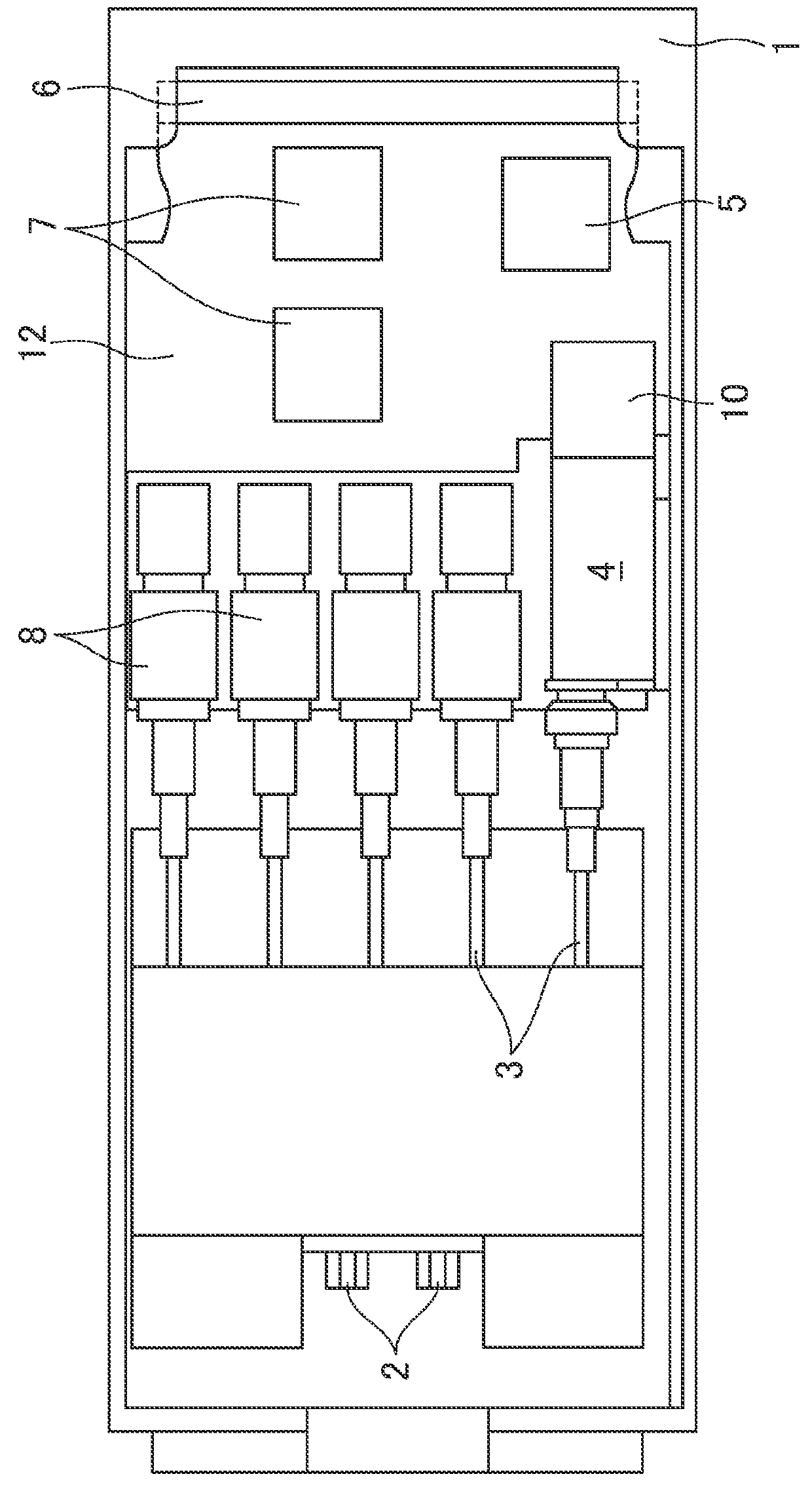
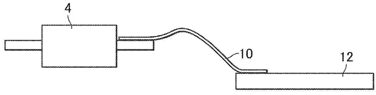
[0059]An optical module using a directly modulated TOSA is not provided with a termination resistor due to a power consumption constraint, and is terminated with an optical semiconductor device having a low resistance value (8 to 12 ohms). Therefore, a high-frequency electric signal is reflected by the optical semiconductor device and travels back toward the second multilayer substrate 12 on which a drive device is mounted. No problem occurs when the reflected wave traveling back toward the second multilayer substrate 12 can be guided to a termination resistor of the drive device without being further reflected by the connection portion of the first multilayer substrate 10 and the second multilayer substrate 12; however, multiple reflection becomes obvious in a high-frequency line when the reflected wave is reflected by the connection portion, which degrades the quality of an optical waveform.

[0060]For 25-GHz high-speed operation, it is necessary to reduce a reflection characteristi...


PUM


Abstract

A first conductive layer includes a first signal wiring including, at a position except for an end portion, a wide portion having a width wider than that of the other portion. A second conductive layer includes a signal electrode electrically continuous with the end portion of the first signal wiring, a first ground plane overlapping the wide portion, and a ground terminal. A third conductive layer includes a second signal wiring including an end portion overlapping and bonded to the signal electrode, and a ground electrode overlapping and bonded to the ground terminal. A fourth conductive layer includes a second ground plane. The second ground plane includes a through hole overlapping the end portion of the second signal wiring. A fifth conductive layer includes a third groundplane. The third groundplane overlaps the end portion of the second signal wiring inside the through hole.

Description

CROSS-REFERENCE TO RELATED APPLICATION[0001]The present application claims priority from Japanese application JP2015-222453 filed on Nov. 12, 2015, the content of which is hereby incorporated by reference into this application.BACKGROUND OF THE INVENTION1. Field of the Invention[0002]The present invention relates to an optical module.2. Description of the Related Art[0003]An optical module has generally a form in which a printed circuit board (hereinafter PCB) on which an optical subassembly, a driver IC that outputs a modulated electric signal, and the like are mounted is included in the interior of the optical module. The housing of the optical subassembly accommodates an optical semiconductor device and is connected with a flexible printed board (hereinafter FPC).[0004]With the widespread use of broadband networks in recent years, an increase in speed, a reduction in size, and a reduction in cost of the optical module are achieved. For reducing the size of the optical module, not...

Claims


Application Information

Patent Timeline
Patent Type & Authority Patents(United States)
IPC IPC(8): G02B6/42G01J1/44
CPCG02B6/428G02B6/4283G02B6/4279G01J1/44H05K1/0274H05K1/115H05K1/147H05K3/363H05K2201/09572
Inventor NOGUCHI, DAISUKEMIZUSEKI, SACHIKOSHIBUYA, NORIMICHIYAMAMOTO, HIROSHI
Owner LUMENTUM JAPAN INC
Why Eureka
Try Eureka