Liquid crystal display device and electronic apparatus having the same

a display device and liquid crystal technology, applied in semiconductor devices, instruments, cathode-ray tube indicators, etc., can solve the problem that the transistor is not necessarily suitable for being formed over a large glass substrate, and achieve the effect of reducing off-state current, improving aperture ratio, and enhancing the added value of the display devi

Active Publication Date: 2018-08-28
SEMICON ENERGY LAB CO LTD
View PDF392 Cites 4 Cited by
  • Summary
  • Abstract
  • Description
  • Claims
  • Application Information

AI Technical Summary

Benefits of technology

[0553]It can be seen from FIG. 28 that in the case of the upper-side layout of the pixel of FIG. 27, the image signal holding period is about 1 minute long. Therefore, at the time of displaying a still image, a constant luminance may be maintained by performing the operation to regularly supply the same image signal (in the diagram, “refresh”). As a result, the length of time to apply a voltage to a transistor included in a driver circuit portion can be drastically shortened. Furthermore, deterioration of a driver circuit over time can be drastically slowed down, which produces advantageous effects such as an improvement in reliability of a liquid crystal display device.
[0554]In Example 2, the results of evaluation of image signal holding characteristics of the liquid crystal display device, which is described in the above embodiment, shown in FIG. 1, and actually manufactured to have a structure which is different from

Problems solved by technology

On the other hand, thin film transistors manufactured using crystalline silicon have high field effect mobility, but due to a crystallization step such as laser annealing, such a transistor is not necessarily suitable for being formed over a large glass substrate.

Method used


Image

  • Liquid crystal display device and electronic apparatus having the same
  • Liquid crystal display device and electronic apparatus having the same
  • Liquid crystal display device and electronic apparatus having the same

Examples


embodiment 1

(Embodiment 1)

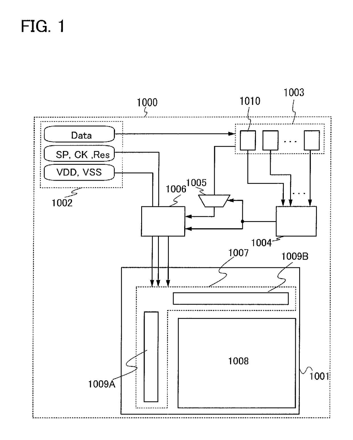
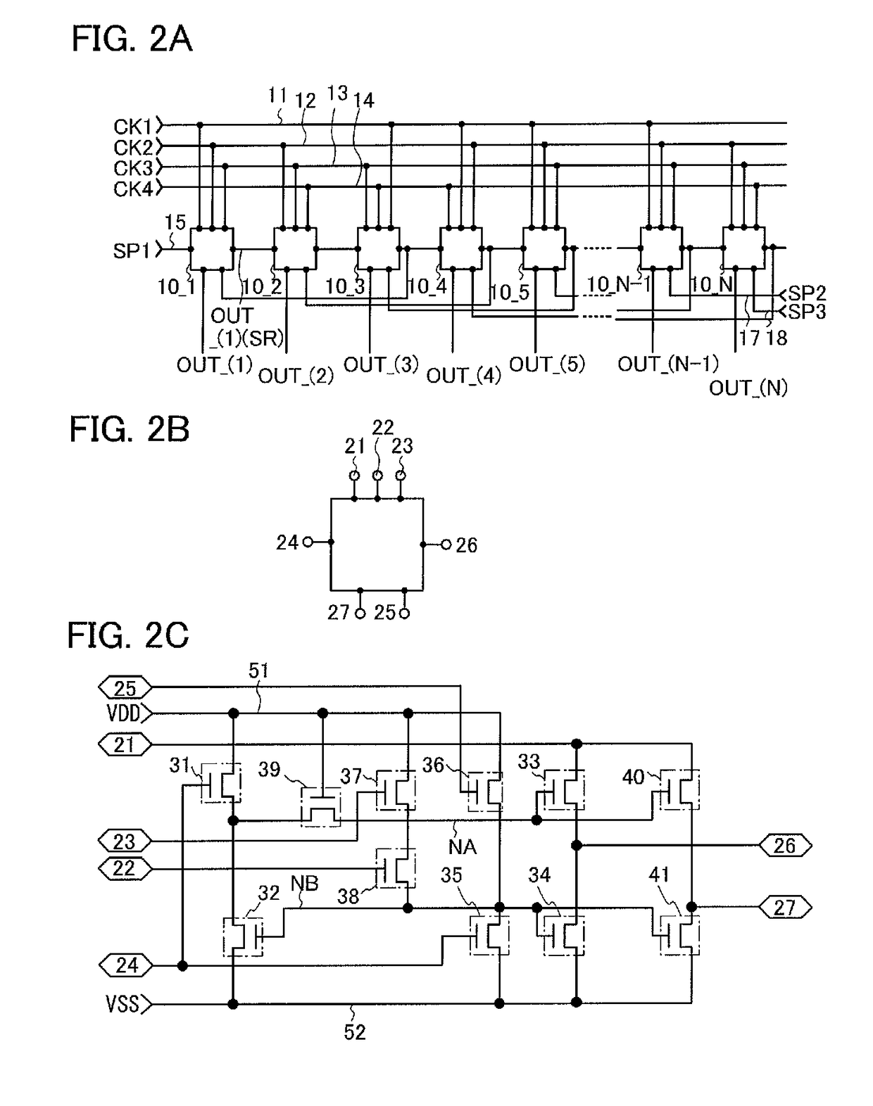
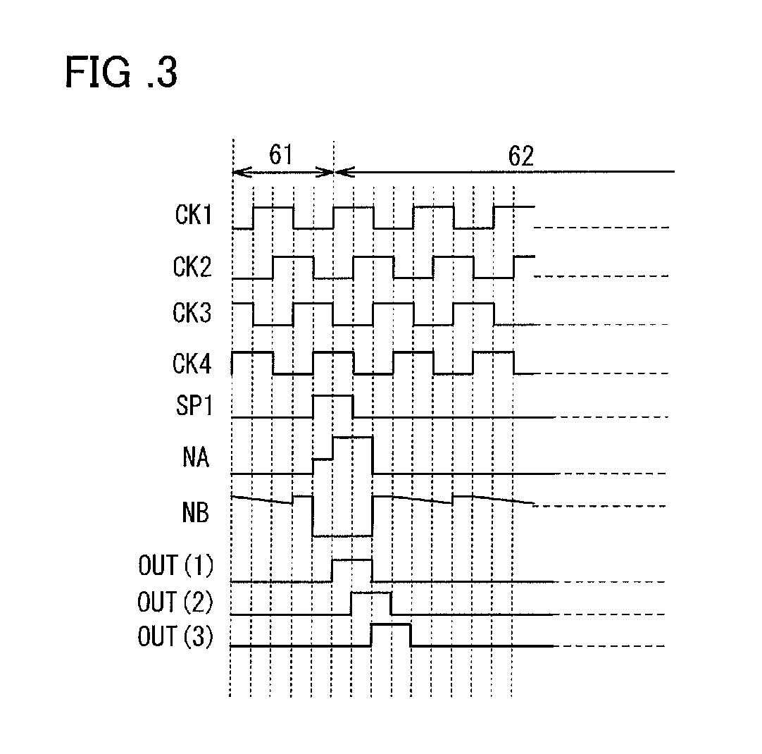
[0054]In this embodiment, a block diagram of a display device and a stop sequence and a start sequence of an operation in a driver circuit are described. First, a block diagram of a display device is described using FIG. 1.

[0055]A liquid crystal display device 1000 described in Embodiment 1 includes a display panel 1001, a signal generation circuit 1002, a memory circuit 1003, a comparison circuit 1004, a selection circuit 1005, and a display control circuit 1006.

[0056]The display panel 1001 includes, for example, a driver circuit portion 1007 and a pixel portion 1008. A gate line driver circuit 1009A and a signal line driver circuit 1009B are included, which are driver circuits for driving the pixel portion 1008 including a plurality of pixels. The gate line driver circuit 1009A, the signal line driver circuit 1009B, and the pixel portion 1008 may be formed using transistors formed over one substrate.

[0057]The gate line driver circuit 1009A, the signal line driver cir...

embodiment 2

(Embodiment 2)

[0128]A thin film transistor of this embodiment and an embodiment of a method for manufacturing the thin film transistor are described using FIGS. 5A and 5B and FIGS. 6A to 6E.

[0129]In Embodiment 2, an example of a thin film transistor which can be applied to a liquid crystal display device described in this specification will be described. A thin film transistor 410 described in Embodiment 2 can be used as a thin film transistor in each pixel of the pixel portion 1008 described in Embodiment 1.

[0130]FIG. 5A illustrates an example of a planar structure of the thin film transistor, and FIG. 5B illustrates an example of a cross-sectional structure thereof. The thin film transistor 410 shown in FIGS. 5A and 5B is a top-gate thin film transistor.

[0131]FIG. 5A is a plane view of the top-gate thin film transistor 410 and FIG. 5B is a cross-sectional view along line C1-C2 in FIG. 5A.

[0132]The thin film transistor 410 includes over a substrate 400 having an insulating surface,...

embodiment 3

(Embodiment 3)

[0198]In Embodiment 3, another example of a thin film transistor which can be applied to a liquid crystal display device disclosed in this specification will be described. Note that Embodiment 2 can be applied to the same portions and the portions and steps having similar functions as / to Embodiment 2, and description thereof is not repeated. Further, a specific description for the same portions is omitted. A thin film transistor 460 described in this embodiment can be used as a thin film transistor in each pixel of the pixel portion 1008 described in Embodiment 1.

[0199]A thin film transistor of this embodiment and an embodiment of a method for manufacturing the thin film transistor are described using FIGS. 7A and 7B and FIGS. 8A to 8E.

[0200]FIG. 7A illustrates an example of a planar structure of the thin film transistor, and FIG. 7B illustrates an example of a cross-sectional structure thereof. The thin film transistor 460 shown in FIGS. 7A and 7B is a top-gate thin f...


PUM

PropertyMeasurementUnit
gate voltageaaaaaaaaaa

Abstract

A liquid crystal display device includes: a driver circuit portion; a pixel portion; a signal generation circuit for generating a control signal for driving the driver circuit portion and an image signal which is supplied to the pixel portion; a memory circuit; a comparison circuit for detecting a difference of image signals for a series of frame periods among image signals stored for respective frame periods in the memory circuit; a selection circuit which selects and outputs the image signals for the series of frame periods when the difference is detected in the comparison circuit; and a display control circuit which supplies the control signal and the image signals output from the selection circuit, to the driver circuit portion when the difference is detected in the comparison circuit, and stops supplying the control signal to the driver circuit portion when the difference is not detected in the comparison circuit.

Description

TECHNICAL FIELD[0001]The present invention relates to liquid crystal display devices. The present invention relates to electronic apparatuses having the liquid crystal display devices.BACKGROUND ART[0002]Thin film transistors formed over a flat plate such as a glass substrate have been manufactured using amorphous silicon, polycrystalline silicon, or the like, as typically seen in liquid crystal display devices. Thin film transistors manufactured using amorphous silicon have low field effect mobility but can be formed over a large glass substrate. On the other hand, thin film transistors manufactured using crystalline silicon have high field effect mobility, but due to a crystallization step such as laser annealing, such a transistor is not necessarily suitable for being formed over a large glass substrate.[0003]In view of the foregoing, attention has been drawn to a technique by which a thin film transistor is manufactured using an oxide semiconductor, and such a transistor is appl...

Claims


Application Information

Patent Timeline
Patent Type & Authority Patents(United States)
IPC IPC(8): G09G3/36G02F1/1368H01L27/12H01L29/786
CPCG02F1/1368G09G3/3674H01L27/1225H01L29/7869G09G2330/022G09G3/3648G09G2320/103G09G2330/021G09G3/3611G09G3/3677G09G5/18G09G2310/0286G09G2330/027H01L29/06
Inventor YAMAZAKI, SHUNPEIKOYAMA, JUNMIYAKE, HIROYUKITSUBUKU, MASASHINODA, KOSEI
Owner SEMICON ENERGY LAB CO LTD
Why Eureka
Try Eureka