Eureka AIR delivers breakthrough ideas for toughest innovation challenges, trusted by R&D personnel around the world.

Semiconductor laser device and method of making the same

a laser device and semiconductor technology, applied in semiconductor lasers, laser details, electrical devices, etc., can solve the problems of inability to design the light output, inability to achieve the light output, and impaired stability of the light emitting pattern, etc., to achieve less temperature difference, good suppression of thermal interference generated between the plurality of waveguide structures, and high thermal conductivity

Active Publication Date: 2018-08-28
ROHM CO LTD
View PDF5 Cites 0 Cited by
  • Summary
  • Abstract
  • Description
  • Claims
  • Application Information

AI Technical Summary

Benefits of technology

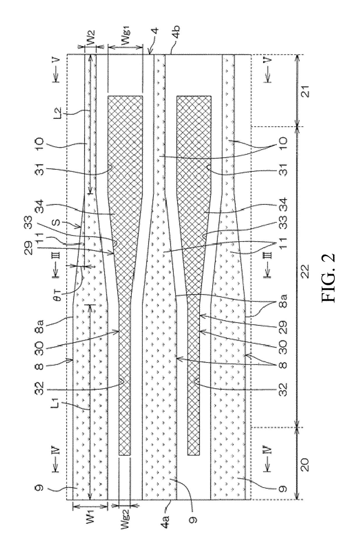
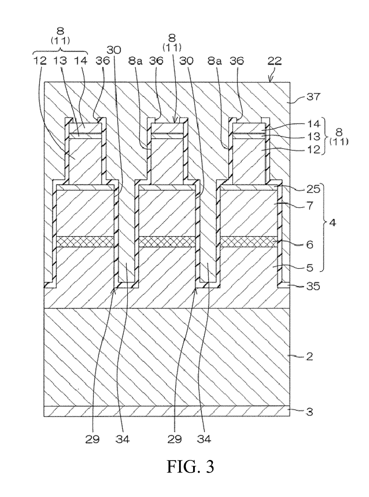
[0007]The semiconductor laser device of the present invention is conFIG.d as the following configuration, i.e. a divider is formed between adjacent waveguide structures for dividing the active layer. The divider comprises a groove for dividing the active layer, and a heat dissipation material filled in the groove and having a thermal conductivity higher than a thermal conductivity of a semiconductor layer. By way of the divider, heat generated from the plurality of waveguide structures is conducted between the waveguide structures, so as to inhibit generation of a temperature difference between the plurality of waveguide structures.
[0008]That is, by way of the divider, the heat generated from the plurality of waveguide structures is dissipated to the outside, and the plurality of waveguide structures can be made close to a soaking state, i.e. a state that there is less temperature difference between the plurality of waveguide structures. Hence, thermal interference generated between the plurality of waveguide structures can be well suppressed. Accordingly, a semiconductor laser device capable of realizing stable light emitting patterns and high output is provided.

Problems solved by technology

However, in the configuration in which a plurality of waveguide structures are disposed, since the plurality of waveguide structures are oscillated at the same time, in the result that heat from one waveguide structure is conducted to adjacent waveguide structures, there is a concern that the waveguide structures reach a high temperature exceeding an operating temperature due to thermal interference.
In addition, when a temperature difference is generated between a plurality of waveguide structures, uneven light output is generated between the plurality of waveguide structures, and as a result, the design of the light output cannot be obtained, and the stability of the light emitting pattern is also impaired.

Method used


Image

  • Semiconductor laser device and method of making the same
  • Semiconductor laser device and method of making the same
  • Semiconductor laser device and method of making the same

Examples


Embodiment Construction

[0026]Hereinafter, embodiments of the present invention will be described in detail with reference to the accompanying drawings.

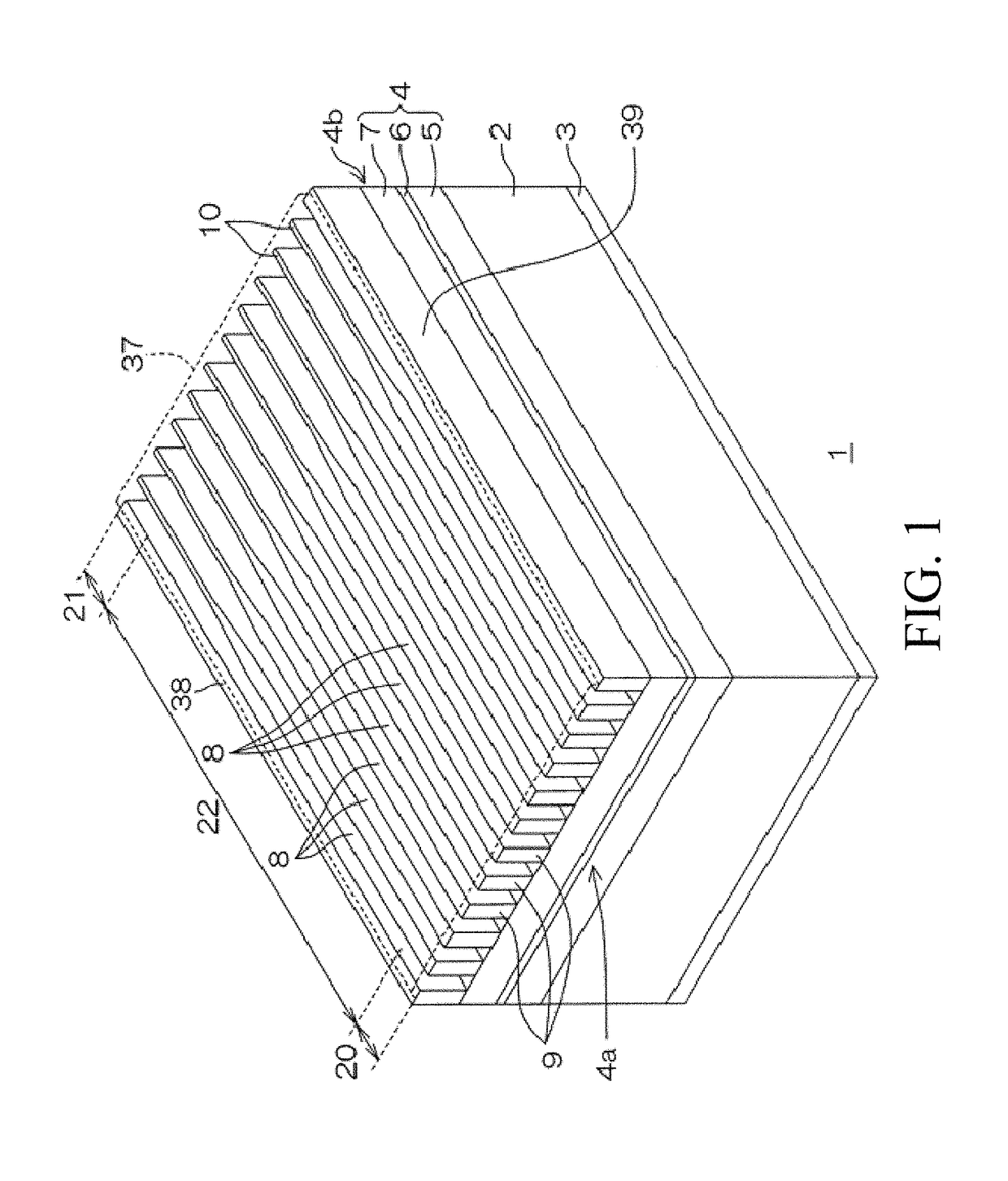
[0027]FIG. 1 is a perspective view showing a semiconductor laser device 1 according to an embodiment of the present invention. FIG. 2 is an enlarged top view showing several waveguide structures 8 shown in FIG. 1. FIG. 3 is a longitudinal cross-sectional view taken along the line III-III shown in FIG. 2. FIG. 4 is a longitudinal cross-sectional view taken along the line IV-IV shown in FIG. 2. FIG. 5 is a longitudinal cross-sectional view taken along the line V-V shown in FIG. 2.

[0028]The semiconductor laser device 1 is, for example, a compound semiconductor laser diode having an operating voltage VOP of 3 V or less and emitting light (laser) having a peak emission wavelength in a range from 700 nm to 1000 nm. The semiconductor laser device 1 comprises an n-type substrate 2. The substrate 2 can be, for example, an n-type GaAs substrate. The substrate 2 is fo...


PUM


Abstract

The present invention provides a semiconductor laser device for improving temperature characteristics of waveguide structures and realizing stable light emitting patterns and high output, and a method for making the same. The semiconductor laser device (1) comprises: an n-type clad layer (5) laminated on a substrate (2); an active layer (6) laminated on the n-type clad layer (5); a p-type clad layer (7) laminated on the active layer (6); and a plurality of waveguide structures (8) formed on the p-type clad layer (7) and having a ridge of a horn shape in top view. In this configuration, a divider (29) is formed between adjacent waveguide structures (8), and the divider (29) comprises: a groove (30) dividing the active layer (6); and a heat dissipation material (34) filled in the groove (30) and having a thermal conductivity higher than a thermal conductivity of a semiconductor layer (4).

Description

BACKGROUND[0001]The present invention relates to a semiconductor laser device and a method of making the same. In recent years, in the field of semiconductor laser devices, it is required that the generated light (laser) is highly outputted, and thus various types are proposed. For example, Patent Literature 1 discloses a semiconductor laser device with a waveguide structure having a ridge of a horn shape in top view as a type in which high output can be realized.PRIOR TECHNICAL LITERATUREPatent Literatures[0002][Patent Literature 1] Japanese Patent Application Laid-Open No. 8-23133BRIEF SUMMARY OF THE INVENTIONProblems to be Solved[0003]In order to realize further high output of a semiconductor laser device, the inventors of the present invention have studied the configuration of a plurality of waveguide structures having ridges of a horn shape in top view on the same substrate. It is considered that the light output can be theoretically increased in proportion to the number of wav...

Claims


Application Information

Patent Timeline
Patent Type & Authority Patents(United States)
IPC IPC(8): H01S5/02H01S5/024H01S5/22H01S5/026
CPCH01S5/026H01S5/22H01S5/02469H01S5/04252H01S5/1014H01S5/2086H01S5/209H01S5/2275H01S5/4031H01S2301/176
Inventor KITAJIMA, HISAYOSHI
Owner ROHM CO LTD
Why Eureka
Eureka Blog
Learn More