Chamfering circuit of adjustable chamfered waveform and adjust method of chamfered waveform

a technology of adjustable chamfering and adjustable chamfering waveform, which is applied in the field of display technology, can solve the problems of low work efficiency and complicated operation of such methods, and achieve the effects of high work efficiency, simple operation and promotion of image quality

Active Publication Date: 2018-09-11
TCL CHINA STAR OPTOELECTRONICS TECH CO LTD
View PDF5 Cites 0 Cited by
  • Summary
  • Abstract
  • Description
  • Claims
  • Application Information

AI Technical Summary

Benefits of technology

[0006]An objective of the present invention is to provide a chamfering circuit of adjustable chamfered waveform, which can conveniently and quickly adjust the chamfered waveform to promote the work efficiency and to improve the image quality.
[0007]Another objective of the present invention is to further provide an adjust method of a chamfered waveform, which can conveniently and quickly adjust the chamfered waveform to promote the work efficiency and to improve the image quality.
[0033]The benefits of the present invention are: the present invention provides a chamfering circuit of adjustable chamfered waveform, comprising a digital power source IC, a first resistor, a second resistor and a triode; wherein the chamfered waveform can be adjusted by adjusting the triode base voltage outputted by the digital power source IC to promote the image quality. In comparison with prior art, welding the resistor is not required to accomplish the adjustment of the chamfered waveform. The operation is simple and the work efficiency is high. The present invention further provides an adjust method of a chamfered waveform, which can conveniently and quickly adjust the chamfered waveform to promote the work efficiency and to improve the image quality.

Problems solved by technology

The operation of such method is complicated and the work efficiency is low.

Method used


Image

  • Chamfering circuit of adjustable chamfered waveform and adjust method of chamfered waveform
  • Chamfering circuit of adjustable chamfered waveform and adjust method of chamfered waveform
  • Chamfering circuit of adjustable chamfered waveform and adjust method of chamfered waveform

Examples


Embodiment Construction

[0042]For better explaining the technical solution and the effect of the present invention, the present invention will be further described in detail with the accompanying drawings and the specific embodiments.

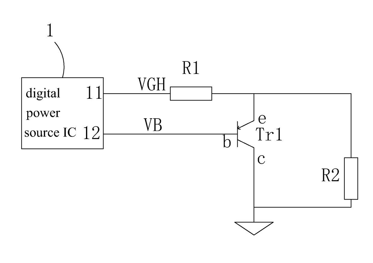
[0043]Please refer to FIG. 3. The present invention provides a chamfering circuit of adjustable chamfered waveform, comprising: a digital power source IC 1, a first resistor R1, a second resistor R2 and a triode Tr1; wherein

[0044]the digital power source IC 1 comprises: a TFT activation voltage output terminal 11 and a triode base voltage output terminal 12;

[0045]one end of the first resistor R1 is electrically coupled to the TFT activation voltage output terminal 11 of the digital power source IC 1, and the other end is electrically coupled to an emitter e of the triode Tr1;

[0046]a base b of the triode Tr1 is electrically coupled to the triode base voltage output terminal 12 of the digital power source IC 1, and the emitter e is electrically coupled to one end of the second r...


PUM


Abstract

The present invention provides a chamfering circuit of adjustable chamfered waveform and an adjust method of a chamfered waveform. The chamfering circuit of adjustable chamfered waveform according to the present invention comprises a digital power source IC (1), a first resistor (R1), a second resistor (R2) and a triode (Tr1); wherein the chamfered waveform can be adjusted by adjusting the triode base voltage (VB) outputted by the digital power source IC (1) to promote the image quality. In comparison with prior art, welding the resistor is not required to accomplish the adjustment of the chamfered waveform. The operation is simple and the work efficiency is high.

Description

FIELD OF THE INVENTION[0001]The present invention relates to a display technology field, and more particularly to a chamfering circuit of adjustable chamfered waveform and an adjust method of a chamfered waveform.BACKGROUND OF THE INVENTION[0002]The LCD (Liquid Crystal Display) possesses many advantages of being ultra thin, power saved and radiation free. It has been widely utilized in, such as LCD TVs, mobile phones, Personal Digital Assistant (PDA), digital cameras, laptop screens or notebook screens, and dominates the flat panel display field.[0003]Most of the liquid crystal displays on the present market are backlight type liquid crystal displays, which comprise a liquid crystal display panel and a backlight module. The working principle of the liquid crystal display panel is that the Liquid Crystal is injected between the Thin Film Transistor Array Substrate (TFT array substrate) and the Color Filter (CF). The light of backlight module is refracted to generate images by applyin...

Claims


Application Information

Patent Timeline
Patent Type & Authority Patents(United States)
IPC IPC(8): G09G3/36H03K5/08
CPCG09G3/3696H03K5/082G09G3/3648G09G2310/06G09G3/3677G09G2310/0286G09G2310/066G09G2320/0219
Inventor FU, WEI
Owner TCL CHINA STAR OPTOELECTRONICS TECH CO LTD
Why Eureka
Try Eureka