Non-destructive 3-dimensional chemical imaging of photo-resist material

a photo-resist material, chemical imaging technology, applied in the direction of optical radiation measurement, instruments, spectrometry/spectrophotometry/monochromators, etc., can solve the problems of high yield loss in substrate package technology development (sptd) or bump-less build-up, and no solution exists in the industry for 3-dimensional (3d) imaging and quantitative characterization of photo-resist materials

Inactive Publication Date: 2018-09-18
INTEL CORP
View PDF7 Cites 0 Cited by
  • Summary
  • Abstract
  • Description
  • Claims
  • Application Information

AI Technical Summary

Problems solved by technology

One of the key issues resulting in high yield loss in substrate package technology development (SPTD) or bump-less build-up layer (BBUL) packaging is unacceptable borders or defective borders (e.g., “border defects”) between regions of light exposed (e.g., cured) and unexposed (e.g., uncured) resist film material.
Currently no solutions exist in the industry for 3-Dimensional (3D) imaging and quantitative characterization of photo-resist during or after exposure to light to cure the material, such as to identify border defects.
This greatly limits process development and optimization for substrate technology development.
Inconsistencies or defects in the exposure lighting, or mask used to expose the exposed regions may be contributors for border defects “hidden defects”.
Such defects can result in inaccurate or unacceptable trace geometry, and thus cause conductive traces to malfunction, short to other traces, or open circuit where contact should exist.
Such defects also can result in smaller contact area between conductive traces and insulating substrate, and thus cause conductive trace to lift off in downstream process.
Such liftoff can result in damaged, destroyed or missing lengths of the conductive traces, often causing undesired open circuits in the trace circuitry.

Method used


Image

  • Non-destructive 3-dimensional chemical imaging of photo-resist material
  • Non-destructive 3-dimensional chemical imaging of photo-resist material
  • Non-destructive 3-dimensional chemical imaging of photo-resist material

Examples


examples

[0092]The following examples pertain to embodiments.

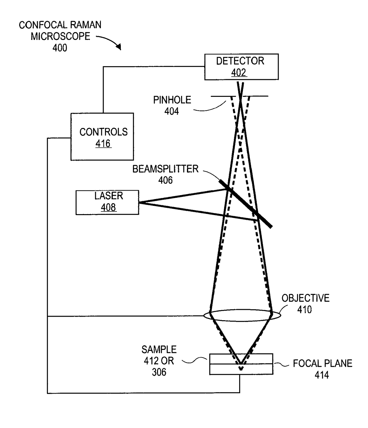
[0093]Example 1 is a method for detecting defects in an border between exposed regions of a photo resist layer and unexposed regions of the photo resist layer comprising: inspecting the layer of photo resist with a confocal Raman microscope, wherein the resist is formed a conductive surface and includes borders between exposed regions of the photo resist layer and unexposed regions of the photo resist layer, wherein inspecting includes chemically identifing the borders between the exposed regions and unexposed regions.

[0094]In Example 2, the subject matter of Example 1 can optionally include, further comprising, prior to inspecting, exposing a layer of photo resist formed on a conductive surface to light to form borders between exposed regions of the photo resist layer and unexposed regions of the photo resist layer.

[0095]In Example 3, the subject matter of Example 1 can optionally include, further comprising, indentifying acceptab...


PUM

PropertyMeasurementUnit
wavelengthaaaaaaaaaa

Abstract

Embodiments include devices, systems and processes for using a combined confocal Raman microscope for inspecting a photo resist film material layer formed on the top surface of a layer of a substrate package, to detect border defects between regions of light exposed (e.g., cured) and unexposed (e.g., uncured) resist film material. Use of the confocal Raman microscope may provide a 3D photo-resist chemical imaging and characterization technique based on combining (1) Raman spectroscopy to identify the borders between regions of light exposed and unexposed resist along XY planes, with (2) Confocal imaging to select a Z-height of the XY planes scanned. Such detection provides fast, high resolution, non-destructive in-line inspection, and improves technical development of polymerization profiles of the resist film material.

Description

BACKGROUND[0001]Field[0002]Embodiments of the invention are related to inspecting a photo resist film material layer, such as formed on the top surface of a conductive layer of a chip package, to detect border defects between regions of light exposed (e.g., cured) and unexposed (e.g., uncured) resist film material.[0003]Description of Related Art[0004]One of the key issues resulting in high yield loss in substrate package technology development (SPTD) or bump-less build-up layer (BBUL) packaging is unacceptable borders or defective borders (e.g., “border defects”) between regions of light exposed (e.g., cured) and unexposed (e.g., uncured) resist film material.[0005]Currently no solutions exist in the industry for 3-Dimensional (3D) imaging and quantitative characterization of photo-resist during or after exposure to light to cure the material, such as to identify border defects. This greatly limits process development and optimization for substrate technology development. Inconsist...

Claims


Application Information

Patent Timeline
Patent Type & Authority Patents(United States)
IPC IPC(8): G01J3/28G01J3/04G01J3/44G01N21/95G01N21/84G01N21/65G02B21/00G01N21/21
CPCG02B21/008G01N21/65G01N21/8422G02B21/0064G01N21/9501G01N2021/656G01J3/44G01N21/21
Inventor GHOSH, NILANJAN Z.MCCARTHY, KEVIN T.WANG, ZHIYONGGOYAL, DEEPAKLIU, CHANGHUAARANA, LEONEL R.
Owner INTEL CORP
Why Eureka
Try Eureka