Touch panel having two transparent conductive layers with different thicknesses and fabrication method thereof

a technology of transparent conductive layer and touch panel, which is applied in the field of touch panel, can solve the problems of negative influence on production yield and reliability, and achieve the effects of avoiding defects of connection electrodes, reducing resistance of other electrodes, and maintaining a relatively low resistance of electrodes

Active Publication Date: 2018-10-23
HENGHAO TECH CO LTD
View PDF11 Cites 0 Cited by
  • Summary
  • Abstract
  • Description
  • Claims
  • Application Information

AI Technical Summary

Benefits of technology

[0005]In the present invention, one of the embodiments provides a method of fabricating a touch panel. A thinner second patterned transparent conductive layer is used to form the connection electrode on the insulating block and a thicker first patterned transparent conductive layer is used to provide relatively lower resistance in other electrodes. Accordingly, defects of the connection electrodes may be avoided while the resistance of the electrodes is still kept in a relatively lower level, and the production yield and reliability may be enhanced too.

Problems solved by technology

However, when a transparent conductive material such us indium tin oxide (ITO) is used to form the connection electrode, a thicker indium tin oxide may be easily effected by external stress and then crack instead, and thus the production yield and the reliability may be affected negatively.

Method used


Image

  • Touch panel having two transparent conductive layers with different thicknesses and fabrication method thereof
  • Touch panel having two transparent conductive layers with different thicknesses and fabrication method thereof
  • Touch panel having two transparent conductive layers with different thicknesses and fabrication method thereof

Examples


Embodiment Construction

[0040]In the following description, numerous embodiments and respective schematic diagrams and specific details are given to provide a further understanding of the present invention.

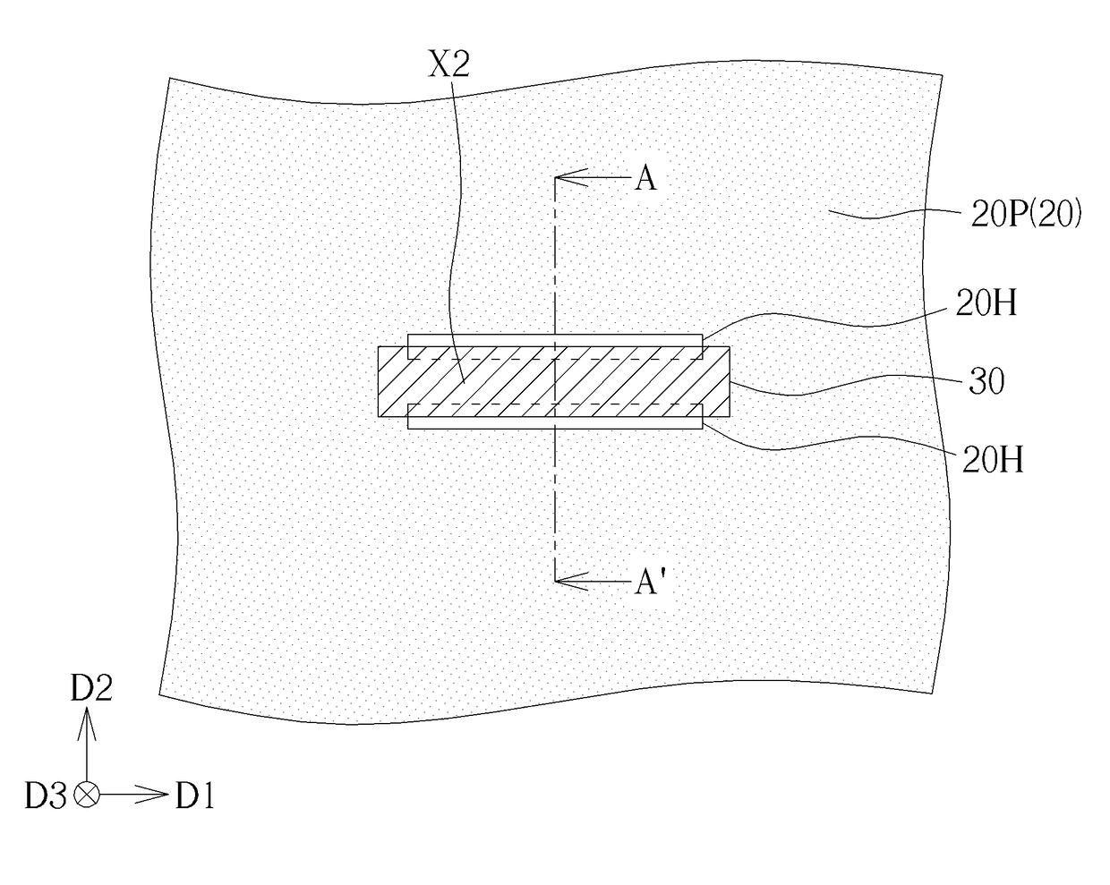
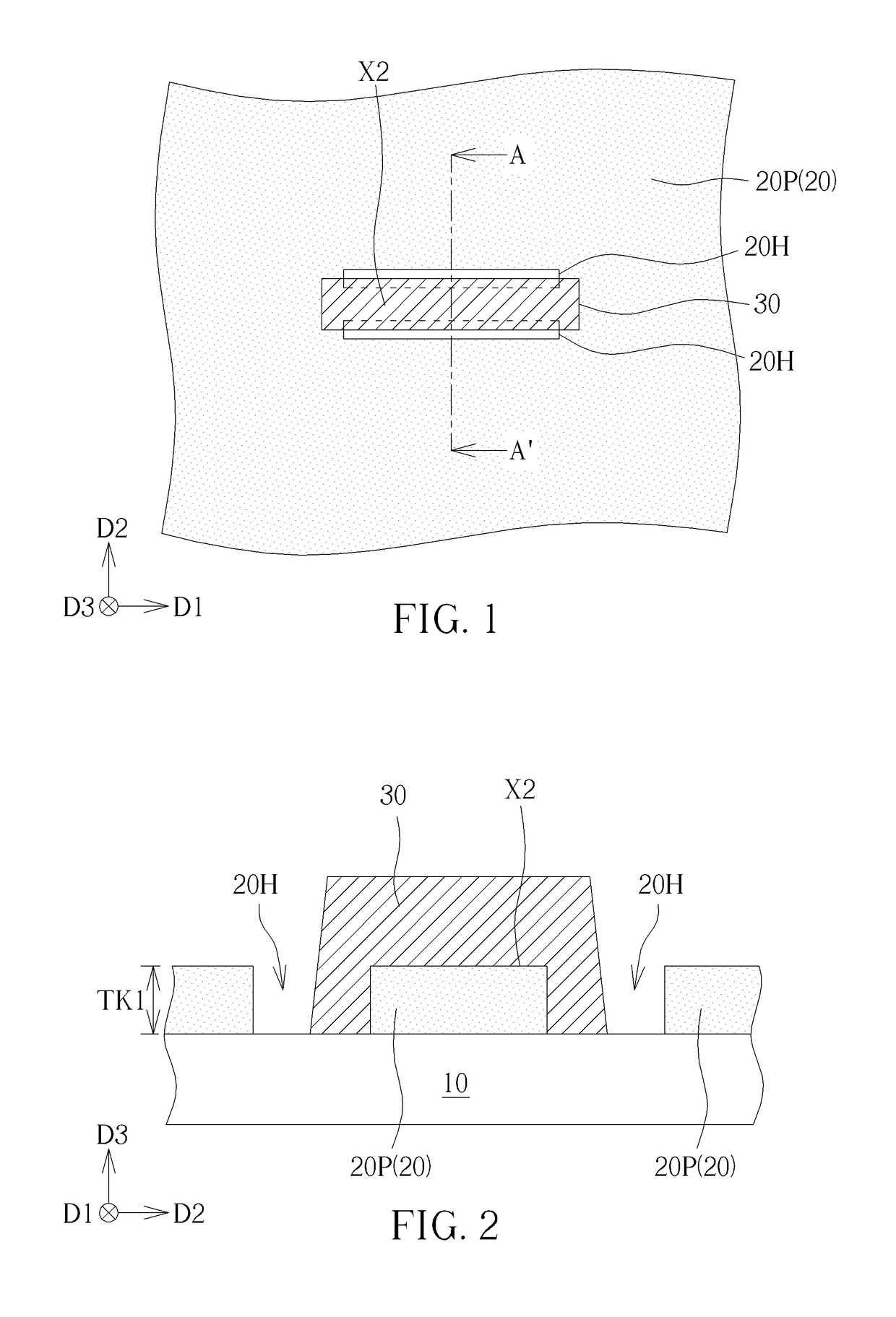
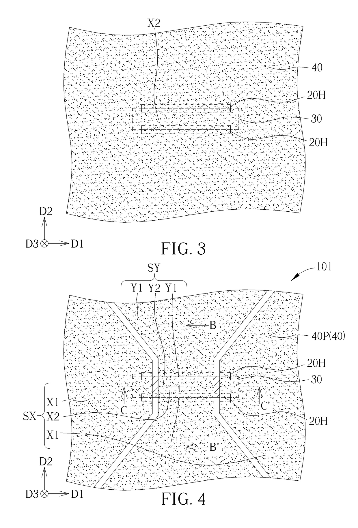
[0041]Please refer to FIGS. 1-6. FIGS. 1-6 illustrate a method of fabricating a touch panel according to a first embodiment of the present invention. For brevity purposes, please note that the figures are only for illustration and the figures may not be to scale. The scale may be further modified according to different design considerations. The method of fabricating the touch panel according to the first embodiment of the present invention includes following steps. First, as illustrated in FIG. 1 and FIG. 2, a first patterned transparent conductive layer 20P is formed on a substrate 10, the first patterned transparent conductive layer 20P includes a plurality of openings 20H. More specifically, to form the first patterned transparent conductive layer 20P, a first transparent conductive layer 20 on the s...


PUM


Abstract

A touch panel includes a substrate, a first patterned transparent conductive layer, at least one insulating block and a second patterned transparent conductive layer. The first patterned transparent conductive layer is disposed on a substrate and includes at least one first connection electrode. The insulating block is disposed on the substrate and at least partially covers the first connection electrode. The second patterned transparent conductive layer is disposed on the insulating block and the first patterned transparent conductive layer. The second patterned transparent conductive layer includes at least one second connection electrode disposed on the insulating block. A thickness of the second patterned transparent conductive layer is smaller than a thickness of the first patterned transparent conductive layer.

Description

BACKGROUND OF THE INVENTION[0001]1. Field of the Invention[0002]The present invention relates to a touch panel and a method of fabricating the same, and more particularly, to a touch panel with connection electrodes in different directions formed by patterned transparent conductive layers of different thicknesses and a method of fabricating the touch panel.[0003]2. Description of the Prior Art[0004]Recently, the touch technology grows rapidly, and many consumer electronics such as mobile phones, GPS navigator systems, tablet PCs, PDAs, laptops and so on with touch sensing functions have been released. The technology of touch panels is variant, and the commonly known touch panels include a resistive touch panel, a capacitive touch panel, an optical touch panel and so on. Additionally, some commonly known electrode structures are bridge type (e.g., SITO), double layer type (e.g., DITO), one layer sensor (OLS) type and so on. In the bridge type touch panel, an insulating block is used ...

Claims


Application Information

Patent Timeline
Patent Type & Authority Patents(United States)
IPC IPC(8): G06F3/041G06F3/044
CPCG06F3/041G06F3/044G06F2203/04111G06F2203/04103G06F3/0443G06F3/0446G06F3/0445
Inventor CHIANG, CHUN-LUNGYUKI, MASANORIWONG, CHING-FANGLU, SHIH-CHUNGYANG, MING-HUNGLIU, CHIN-CHANG
Owner HENGHAO TECH CO LTD
Why Eureka
Try Eureka