Solid-state image sensor and camera

a solid-state image sensor and camera technology, applied in the field of solid-state image sensors and cameras, can solve problems such as reducing light collection efficiency, and achieve the effect of improving light collection efficiency

Active Publication Date: 2018-10-30
CANON KK
View PDF14 Cites 1 Cited by
  • Summary
  • Abstract
  • Description
  • Claims
  • Application Information

AI Technical Summary

Benefits of technology

[0006]The present invention provides a technique advantageous in improving light collection efficiency.

Problems solved by technology

This may reduce light collection efficiency.

Method used


Image

  • Solid-state image sensor and camera
  • Solid-state image sensor and camera
  • Solid-state image sensor and camera

Examples


Embodiment Construction

[0017]Exemplary embodiments of the present invention will be described below with reference to the accompanying drawings.

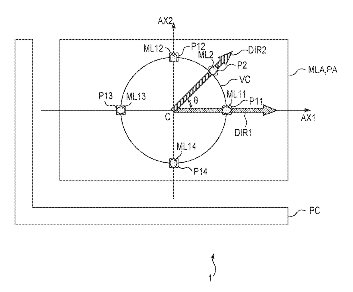
[0018]FIG. 1 shows the arrangement of a solid-state image sensor 1 according to an embodiment of the present invention. The solid-state image sensor 1 includes a microlens array MLA in which a plurality of microlenses are arrayed so as to constitute a plurality of rows and a plurality of columns. From another viewpoint, the solid-state image sensor 1 includes a pixel array PA in which a plurality of pixels each including the microlens are arrayed so as to constitute the plurality of rows and the plurality of columns. Each pixel which constitutes the pixel array PA includes, in addition to the microlens, a photoelectric converter such as a photodiode. Each pixel can also include a color filter. Each pixel can further include a circuit in pixel configured to read out a signal from the photoelectric converter. Each circuit in pixel can include, for example, an amplif...


PUM


Abstract

An image sensor includes microlens array having microlenses arranged to constitute rows and columns. When first axis parallel to the rows and passing through array center of the microlens array, and second axis parallel to the columns and passing through the array center are defined, microlens positioned on virtual circle having the array center as center includes first microlens positioned on the first or second axis, and second microlens positioned on neither the first axis nor the second axis. The first and second microlens have non-circular bottom shape, and width of the second microlens in second direction passing through the second microlens and the array center is larger than width of the first microlens in first direction passing through the first microlens and the array center.

Description

BACKGROUND OF THE INVENTION[0001]Field of the Invention[0002]The present invention relates to a solid-state image sensor and a camera.[0003]Description of the Related Art[0004]Japanese Patent Laid-Open No. 2007-335723 describes a non-circular microlens. More specifically, Japanese Patent Laid-Open No. 2007-335723 describes a solid-state image sensing element which arranges a microlens having an almost circular shape in a plan view in the central portion of a light-receiving region and arranges a microlens having a teardrop shape in a portion away from the central portion of the light-receiving region. The teardrop shape has a long axis and a short axis, and its portion having the maximum width in a direction parallel to the short axis is close to a central portion side in the light-receiving region (FIG. 2, and paragraphs 0021 and 0022 of Japanese Patent Laid-Open No. 2007-335723). The direction of the long axis matches a direction of a straight line passing through the central port...

Claims


Application Information

Patent Timeline
Patent Type & Authority Patents(United States)
IPC IPC(8): G02B3/00H04N5/378H04N5/374H01L27/146
CPCG02B3/0043G02B3/0056H01L27/14627H04N5/374H04N5/378H01L27/14685G02B2003/0093H04N23/54H04N23/55H04N25/71H04N25/76H04N25/75G02B5/021G02B3/0006H04N25/00H01L27/146
Inventor KAWABATA, KAZUNARI
Owner CANON KK
Why Eureka
Try Eureka