Liquid crystal display device

a liquid crystal display and display panel technology, applied in non-linear optics, instruments, optics, etc., can solve the problems of insufficient space for a grounding electrode pattern in the recent thin-frame display device, and the structure fails to provide greater flexibility in designing micro-display panels and thin-frame display panels. to achieve the effect of reducing the frame width reducing the weakening of the resistance of the liquid crystal display devi

Active Publication Date: 2019-01-01
TRIVALE TECH
View PDF14 Cites 0 Cited by
  • Summary
  • Abstract
  • Description
  • Claims
  • Application Information

AI Technical Summary

Benefits of technology

[0011]The present invention has objects to minimize a weakening of resistance of a liquid crystal display device to static electricity and to reduce a frame width of the liquid crystal display device.
[0014]The identification mark, which is no longer used after the shipment of the display device, doubles as the grounding electrode and accordingly eliminates the need for another grounding electrode on the terminal area of the TFT substrate. Using this structure one can obtain a thin-frame liquid crystal display device.
[0015]If electric charge associated with static electricity enters the conductive member or the surface of the color filter, the electric charge would be inhibited from entering the display area and would be discharged through the identification mark that is located on the terminal area of the TFT substrate and is not electrically connected with the display area. This can minimize a weakening of resistance of the liquid crystal display device to static electricity.

Problems solved by technology

Many recent thin-frame display devices have failed to leave sufficient space for a pattern of the grounding electrode, which is to be formed separately from patterns of the above-mentioned components and is to be designed specifically for an electrical connection with a transparent conductive film located on the upper surface of a color filter substrate.
This structure fails to provide greater flexibility in designing micro-display panels and thin-frame display panels.
However, recent liquid crystal display devices have stringent design requirements due to the trend toward thin-frame display devices, and thus, the above technique disclosed in Japanese Patent Application Laid-Open No. 2008-145686 may not meet the requirements.

Method used


Image

  • Liquid crystal display device
  • Liquid crystal display device
  • Liquid crystal display device

Examples


embodiment

Preferred Embodiment

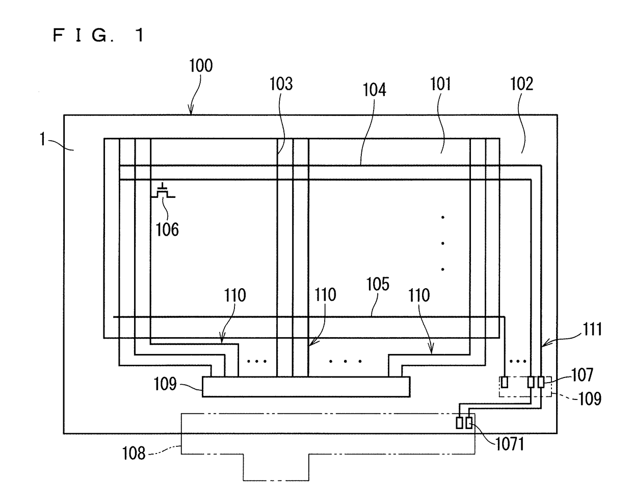
[0026]The following will describe a preferred embodiment of the present invention with reference to the drawings. FIG. 1 is a plan view of a wiring structure of a liquid crystal display device according to the preferred embodiment. All of the accompanying drawings are merely schematic illustrations and do not necessarily reflect, for example, the exact size of each constituent component. For easy understanding, each drawing eliminates or simplifies part of the configuration except for the main constituent components of the present invention.

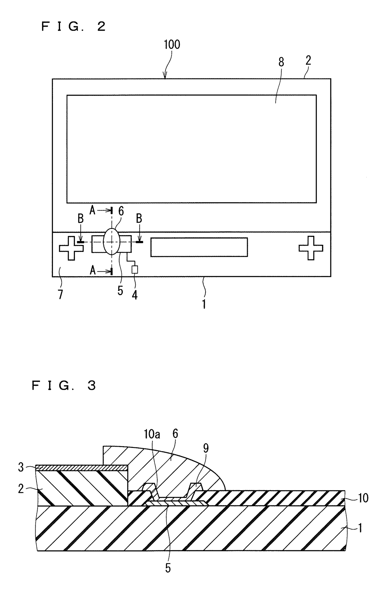
[0027]The wiring structure of the liquid crystal display device will now be described. As illustrated in FIG. 1, the wiring structure of the liquid crystal display device is included in a liquid crystal display panel 100, which is a main constituent component of the liquid crystal display device. FIG. 1 eliminates a color filter substrate 2 (see FIG. 2), which will be described below, to make the wiring structure visible. The ...


PUM

PropertyMeasurementUnit
transparentaaaaaaaaaa
conductiveaaaaaaaaaa
transparent conductiveaaaaaaaaaa

Abstract

A liquid crystal display device includes a TFT substrate, a color filter substrate, liquid crystals, a transparent conductive film, a panel identification pad, and conductive paste. The color filter substrate is opposed to the TFT substrate and has a color filter. The liquid crystals are sealed between the TFT substrate and the color filter substrate. The transparent conductive film is located on a front surface side of the color filter substrate including a periphery of the color filter substrate. The panel identification pad is located on a terminal area that is a portion of the TFT substrate extending beyond the color filter substrate. The panel identification panel is conductive and connected to a ground potential. The conductive paste electrically connects the panel identification pad with the transparent conductive film located on the periphery of the color filter substrate.

Description

BACKGROUND OF THE INVENTION[0001]Field of the Invention[0002]The present invention relates to liquid crystal display devices.[0003]Description of the Background Art[0004]Electro-optical display devices, or, liquid crystal display devices that employ the in-plane switching (IPS) or the fringe field switching (FFS) in particular need to dissipate electric charge on a display surface of a display panel in order to avoid degradation of display quality. For example, as described in Japanese Patent Application Laid-Open No. 2008-145462, such a device typically includes a conductive tape or conductive paste to electrically connect an electrode located on a TFT substrate with the display surface of the display panel.[0005]The device described in Japanese Patent Application Laid-Open No. 2008-145462 includes, in a terminal area, not only a grounding electrode but also components such as an ID pad, a discrimination mark, a driver IC, and a flexible printed circuit (FPC). Many recent thin-fram...

Claims


Application Information

Patent Timeline
Patent Type & Authority Patents(United States)
IPC IPC(8): G02F1/1368G02F1/1333G02F1/1362G02F1/1335G02F1/1339G02F1/1343
CPCG02F1/136204G02F1/1339G02F1/1368G02F1/133345G02F1/134363G02F1/133514G02F2001/134372G02F1/134336G02F1/136286G02F1/134372
Inventor HIRATA, NAOYAUENO, TAKAHIRO
Owner TRIVALE TECH
Why Eureka
Try Eureka