Semiconductor device and method of manufacturing the semiconductor device

a semiconductor and semiconductor technology, applied in the direction of semiconductor devices, basic electric elements, electrical equipment, etc., can solve the problems of limited integration density of 2d memory devices, limited reliability of device characteristics, and high cost of 3d semiconductor memory devices, so as to improve connection structure

Active Publication Date: 2019-03-12
SAMSUNG ELECTRONICS CO LTD
View PDF22 Cites 12 Cited by
  • Summary
  • Abstract
  • Description
  • Claims
  • Application Information

AI Technical Summary

Benefits of technology

[0005]Exemplary embodiments of the present inventive concept may provide 3D semiconductor memory devices capable of improving a connection structure between a lower channel structure and an upper channel structure.
[0006]Exemplary embodiments of the present inventive concept may provide methods of manufacturing a 3D semiconductor memory device capable of simplifying manufacturing processes.

Problems solved by technology

However, since extremely high-priced apparatuses may be needed to form fine patterns, the integration density of 2D memory devices may be limited by costs.
However, production of 3D semiconductor memory devices may be expensive as compared with 2D semiconductor memory devices and may have limitations regarding providing reliable device characteristics.

Method used


Image

  • Semiconductor device and method of manufacturing the semiconductor device
  • Semiconductor device and method of manufacturing the semiconductor device
  • Semiconductor device and method of manufacturing the semiconductor device

Examples


Embodiment Construction

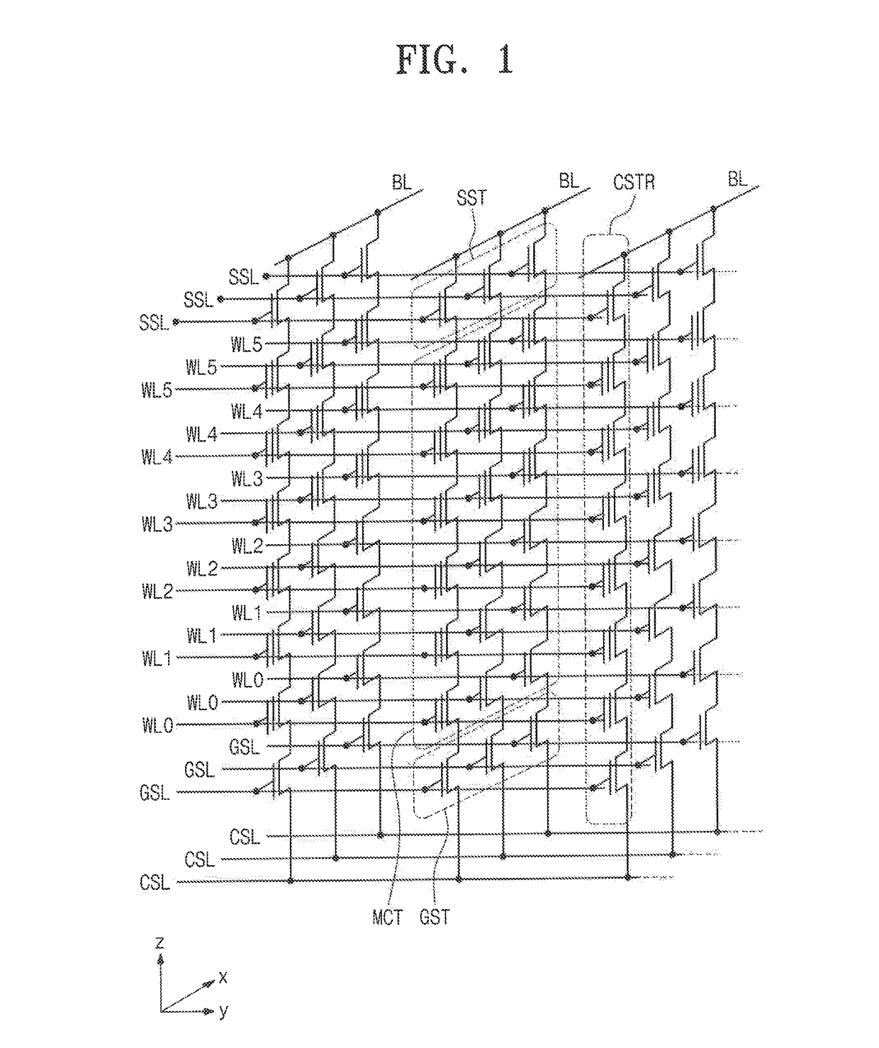
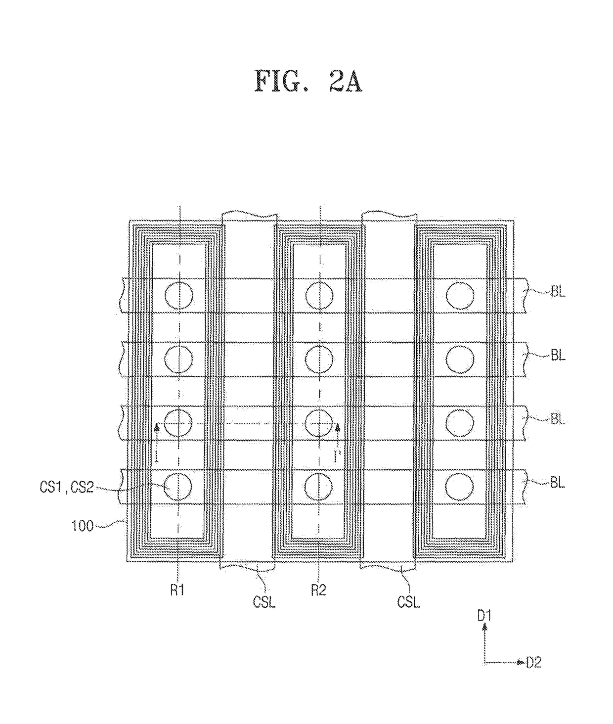
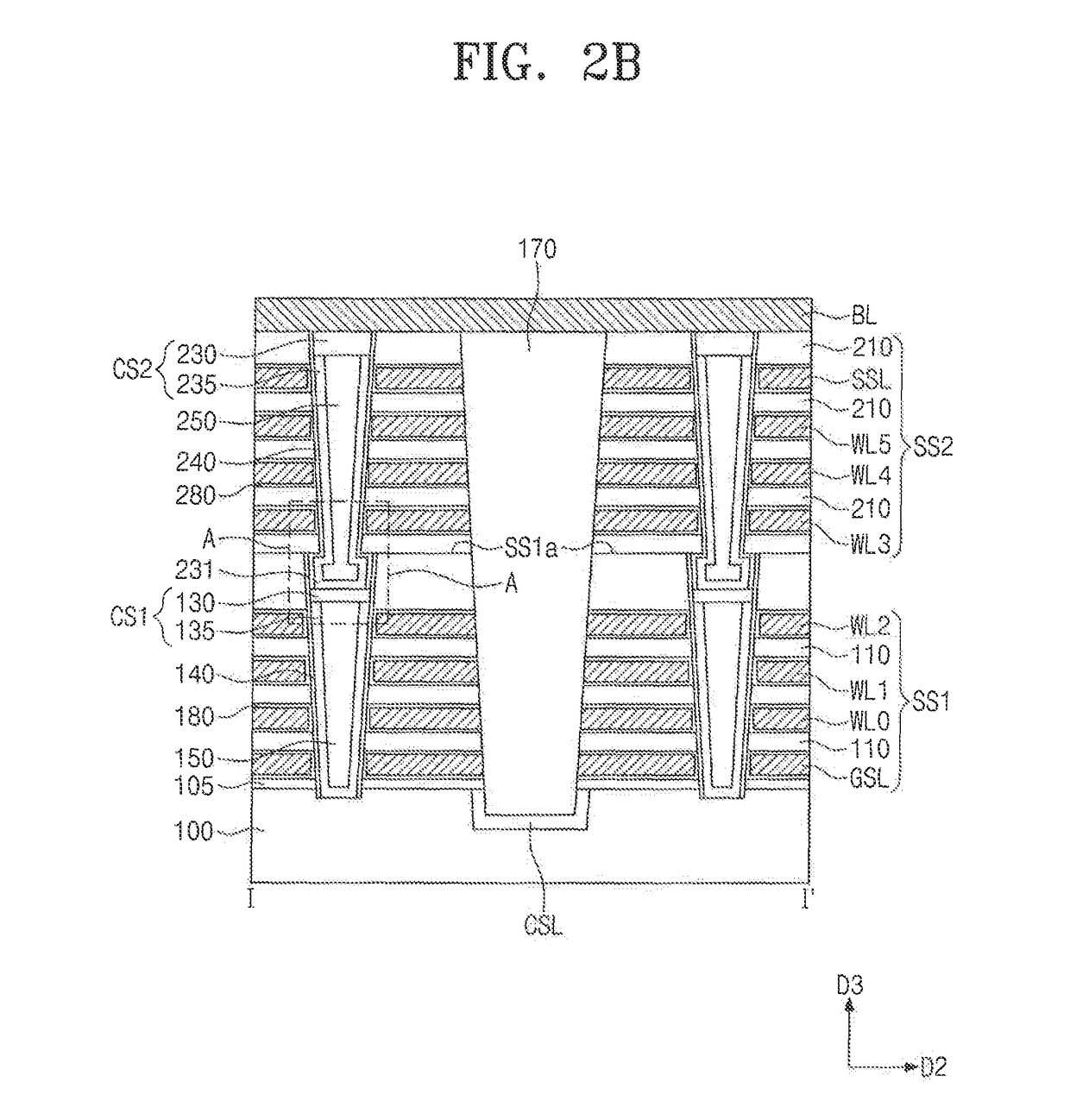
[0042]Exemplary embodiments of the present inventive concept will now be described more fully hereinafter with reference to the accompanying drawings, in which exemplary embodiments of the present inventive concept are shown. Aspects and features of the present inventive concept and methods of achieving them will be apparent from the following exemplary embodiments that will be described in more detail with reference to the accompanying drawings. It should be noted, however, that the present inventive concept is not limited to the following exemplary embodiments, and may be implemented in various forms. In the drawings, exemplary embodiments of the present inventive concept are not limited to the specific examples provided herein, which may be exaggerated for clarity.

[0043]The terminology used herein is for the purpose of describing particular embodiments only and is not intended to limit the exemplary embodiments of the present inventive concept. It will be understood that when an ...


PUM


Abstract

A semiconductor device includes a lower stack structure including lower gate electrodes and lower insulating layers that are alternately and repeatedly stacked on a substrate. The semiconductor device includes an upper stack structure including upper gate electrodes and upper insulating layers that are alternately and repeatedly stacked on the lower stack structure. A lower channel structure penetrates the lower stack structure. An upper channel structure penetrates and is connected to the upper stack structure. A lower vertical insulator is disposed between the lower stack structure and the lower channel structure. The lower channel structure includes a first vertical semiconductor pattern connected to the substrate, and a first connecting semiconductor pattern disposed on the first vertical semiconductor pattern. The upper channel structure includes a second vertical semiconductor pattern electrically connected to the first vertical semiconductor pattern with the first connecting semiconductor pattern disposed therebetween.

Description

CROSS-REFERENCE TO RELATED APPLICATION[0001]This U.S. non-provisional patent application claims priority under 35 U.S.C. § 119 to Korean Patent Application No. 10-2014-0081956, filed on Jul. 1, 2014, in the Korean Intellectual Property Office, the disclosure of which is incorporated by reference herein in its entirety.TECHNICAL FIELD[0002]Exemplary embodiments of the present inventive concept relate to a semiconductor device and a method of manufacturing the semiconductor device.DISCUSSION OF RELATED ART[0003]Semiconductor devices are becoming more highly integrated to provide high performance and low costs. A degree of integration of a two-dimensional (2D) or planar memory device may be determined by an area which a unit memory cell occupies. Therefore, the integration density of the 2D memory device may be affected by a technique of forming fine patterns. However, since extremely high-priced apparatuses may be needed to form fine patterns, the integration density of 2D memory devi...

Claims


Application Information

Patent Timeline
Patent Type & Authority Patents(United States)
IPC IPC(8): H01L27/115H01L27/11582H01L29/10H01L29/792H01L27/1157
CPCH01L27/11582H01L29/7926H01L29/1033H01L27/1157H10B43/35H10B43/27H01L29/78696H01L29/78606
Inventor LEE, DOHYUNLEE, JAEGOOKWON, YOUNG-JINPARK, YOUNGWOOLEE, JAEDUK
Owner SAMSUNG ELECTRONICS CO LTD
Why Eureka
Try Eureka