Tunnel transistor

a tunneling transistor and tunneling technology, applied in the field of tunneling field effect transistors, can solve the problems of overlay/misalignment problems, difficult to form different source and drain regions with a small gate length, etc., and achieve the effect of greater transistor density

Inactive Publication Date: 2019-03-19
ELPIS TECH INC
View PDF27 Cites 20 Cited by
  • Summary
  • Abstract
  • Description
  • Claims
  • Application Information

AI Technical Summary

Benefits of technology

[0008]Techniques and devices as disclosed herein can provide substantial beneficial technical effects. By way of example only and without limitation, one or more embodiments may provide one or more of the following advantages:[0009]Precise overlay of source / drain patterning mask over a small gate not required;[0010]Self-aligned sidewall image transfer (SIT) process enables asymmetry;[0011]Small gate lengths and heterojunctions;[0012]Source and drain contacts formed using different materials, allowing contact resistances between the contacts and the source and drain to be independently minimized;[0013]Different dielectric caps formed on source, drain and gate, enabling wiring common terminals together with one contact wiring and thereby allowing greater transistor density.
[0009]Precise overlay of source / drain patterning mask over a small gate not required;
[0012]Source and drain contacts formed using different materials, allowing contact resistances between the contacts and the source and drain to be independently minimized;
[0013]Different dielectric caps formed on source, drain and gate, enabling wiring common terminals together with one contact wiring and thereby allowing greater transistor density.

Problems solved by technology

However, given the TFET requirements of different source and drain polarities, it can be challenging to form the different source and drain regions with a small gate length.
Such an approach may create overlay / misalignment problems, particularly in devices having relatively small gate lengths.

Method used


Image

  • Tunnel transistor
  • Tunnel transistor
  • Tunnel transistor

Examples


Embodiment Construction

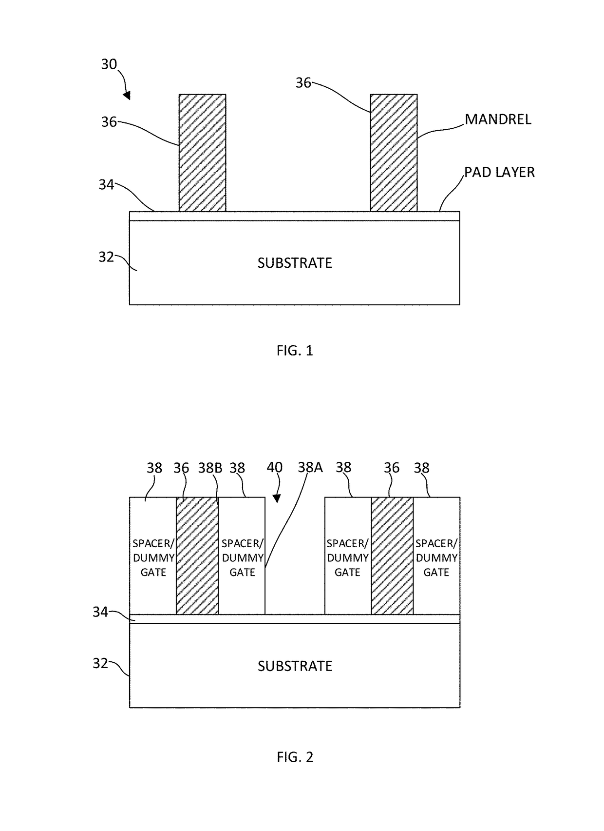
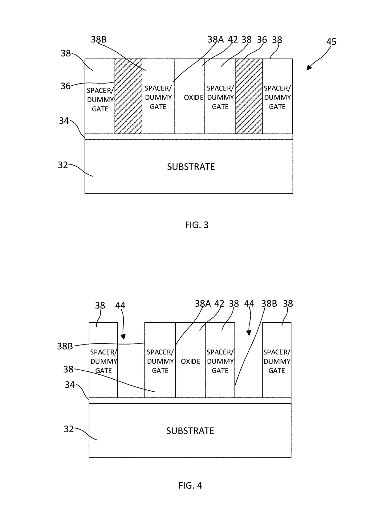
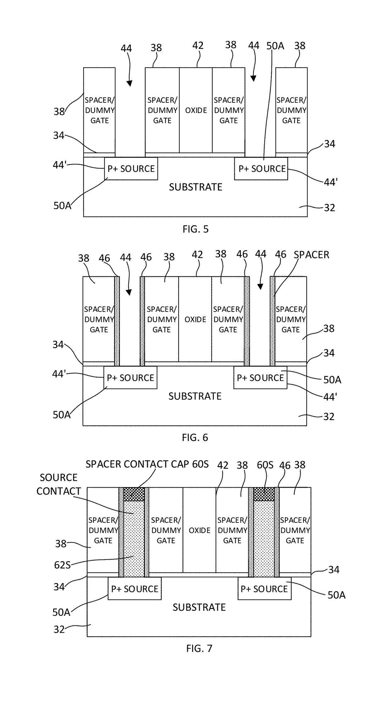
[0032]Principles of the present invention will be described herein in the context of an illustrative tunnel field-effect transistor fabricated on a silicon substrate. It is to be appreciated, however, that the specific embodiments and / or methods illustratively shown and described herein are to be considered exemplary as opposed to limiting. Moreover, it will become apparent to those skilled in the art given the teachings herein that numerous modifications can be made to the embodiments shown that are within the scope of the claims. That is, no limitations with respect to the embodiments shown and described herein are intended or should be inferred.

[0033]The figures schematically illustrate an exemplary sequence of fabrication steps that may be employed in obtaining a tunnel field-effect transistor (TFET). Although the overall fabrication method and the structures formed thereby are novel, certain individual processing steps required to implement the method may utilize conventional s...


PUM


Abstract

A tunnel field-effect transistor having source and drain contacts made from different electrically conductive materials enables independent optimization of contact resistance on the source and drain sides of the transistor. Dielectric caps on the gate electrode, source contact and drain contact made from different materials allow the selective removal of portions of the caps during gate, source and drain wiring. A wiring strap can be formed across the gate and drain to electrically connect two source contacts together. Multiple drain contacts or multiple gate electrodes may alternatively be electrically connected by wiring straps. Strap wiring facilitates placing transistors in closer proximity to increase the number of transistors for a given chip area.

Description

BACKGROUND[0001]The present invention relates generally to the electronic arts and, more particularly, to tunnel field-effect transistors (TFETs) and their fabrication.[0002]Tunnel field-effect transistors are similar in structure to metal oxide semiconductor field-effect transistors (MOSFETs), but require asymmetric source and drain regions that have opposite conductivity types. One conventional TFET device structure contains a P-I-N (p-type-intrinsic-n-type) junction, where the electrostatic potential of the intrinsic region is controlled by a gate terminal. By forming TFET heterojunctions using different materials, TFET performance can be improved.[0003]TFETs have the potential to serve as a viable option for extremely low power applications. However, given the TFET requirements of different source and drain polarities, it can be challenging to form the different source and drain regions with a small gate length. The use of conventional photolithography may involve patterning one...

Claims


Application Information

Patent Timeline
Patent Type & Authority Patents(United States)
IPC IPC(8): H01L21/336H01L21/84H01L29/78H01L29/08H01L23/528H01L21/768H01L29/45H01L29/66
CPCH01L29/66977H01L29/452H01L23/528H01L29/456H01L21/76816H01L21/76897H01L29/66545H01L29/0847H01L29/785H01L21/76877H01L21/845H01L29/41791H01L29/66795H01L29/0692H01L29/7391H01L29/66356H01L29/417H01L29/401H01L21/76895H01L21/76834
Inventor CHENG, KANGGUOXU, PENGWU, HENGBI, ZHENXING
Owner ELPIS TECH INC
Why Eureka
Try Eureka