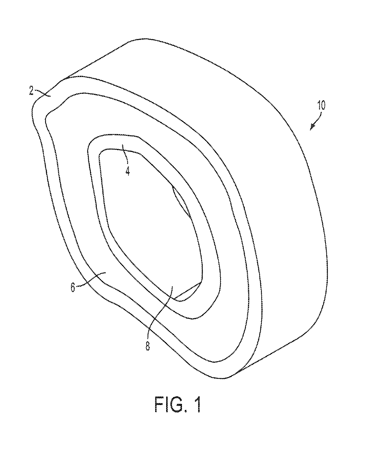
[0006]The present invention addresses such limitations and drawbacks of the prior art by providing a waveguide antenna assembly and process which is conformable to an electronic device, preferably for communications, for transceiving signals of a predetermined radio frequency range comprising a first conductive layer configured in a conformable loop, wherein the first conductive layer has an inner surface and an outer surface, the inner surface and outer surface having an area coextensively disposed between an outer edge and an opposing inner edge; a second conductive layer configured in a conformable loop, having of an area coextensively disposed between an outer edge and an opposing inner edge, wherein the second conductive layer is collaterally aligned with the inner surface of the first conductive layer so as to electrically isolate the second conductive layer from the first conductive layer for support of waveguide modes of the predetermined frequency range; an electrically isolating channel extending between the inner surface of the first conductive layer and the second conductive layer, wherein the electrically isolating channel is dimensionally configured for transmission of the waveguide modes of the predetermined frequency range; an aperture for electromagnetically transceiving the signals, wherein the aperture is coextensively overlayed on a surface of the electrically isolating channel such that opposing sides of the aperture extend between the outer edge of the inner surface of the first conductive layer and the second conductive layer; a back short spaced back from the aperture a predetermined distance equal to a resonant length of the waveguide mode wavelength, wherein the back short provides a circuit impedance between the first conductive layer and the second conductive layer for tuning the waveguide to transceive the signals; and at least one excitation point coupled to the aperture to propagate waveguide modes within the electrically isolating channel supported by a mode barrier filter for reducing internal transmission coupling between the plurality of excitation points so as to transfer excitation point energy to waveguide modes propagated within the electrically isolating channel.
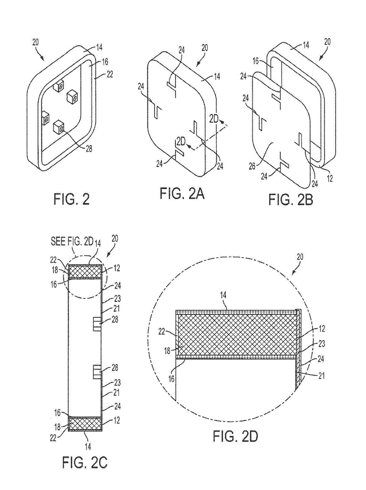
[0016]As further described below, the conformability of the present waveguide's conductive layer imparts adaptability to diverse shapes and sizes and physical configurations wherein they may be fitted within, around or on variously shaped electronic devices supported thereby. Such conformability enables adaptability to underlying device package redesigns without compromising specification-compliant performance, particularly within physical confines of small and compact modern devices, comprises one of many advantages provided by the present waveguide assembly and process. Exemplary geometric configurations, as further described below, include waveguide antenna assemblies which encompass, embed or attach to an electronic device coated by a nonconductive, polymeric material.
[0024]Attributes and properties of the present invention provide many advantages over prior art antennas. First, the internal cavity resonator addresses problems related to detuning through coupling with the technology device, so that antenna performance is not impacted, as open resonators (PIFA, loop, etc) do in compact technology. Second, the present waveguide antenna assembly and system is adaptable to the package surface as an efficient surface wave exciter, allowing previously unused package area (outer surface) to render useful in radiation coverage. Third, the present invention provides a multimode antenna that can be dynamically configured to redirect the antenna radiation pattern or polarization through a combination of precisely excited waveguide modes. Fourth. this invention enables radiation redirection, which is commonly referred to in the art as beam steering, by a single antenna resulting from redirection of the mode(s) formed in a single aperture by the excitation points as specified herein, providing a substantial advantage over arrays of multiple antennas required to redirect radiation patterns in the prior art. Fifth, the multimode reception of the present waveguide antenna assembly and system allows for coherent integration of the one or more excitation points that can be post processed for noise reduction. Sixth, the present waveguide antenna forms an intrinsic EMI barrier, eliminating the need for such shielding. Seventh, the present waveguide antenna with the mode barrier filter, provides a means to isolate the excitation points so that the signals are transceived into antenna modes and not coupled into unwanted transmission modes between excitation points. A yet further, eighth, advantage provided by the present invention is the minimal physical size of the antenna allowing for more compact designs of modern electronic device.
[0025]Such attributes and properties provide many advantages over prior art antennas. An advantage provided by the present invention relates to adaptability of the present waveguide antenna to the exterior surface of an electronic device so as to enhance the resultant radiation pattern. For example, where the electronic device is enclosed in a conductive skin that encompasses a rotational surface (i.e., cylinder, tube, etc.), it is possible to establish surface wave propagation on that conductive skin. In addition, because the natural mode of propagation is similar in field structure to that established by the aperture field, corresponding surface waves are readily excited. Moreover, the adjacent surface of an electronic device may be designed to enhance its interaction with the waveguide antenna to improve those radiation characteristics.
[0026]Substantial advantages provided by the present waveguide antenna assembly and system derive from its compact and versatile geometric configuration. Such conformable size and shape render it adaptable for incorporation into condensed designs for wireless electronic devices which are small, sleek, ergonomic, turnkey, portable assemblies and readily secured to a relevant wearable or other surface. The present waveguide assembly and system thus delivers enhanced electronic performance within size and configuration confines imposed by such compact electronic devices.
