
Organic EL device, method of manufacturing organic EL device, and electronic device

a technology of organic el and el, which is applied in the direction of organic semiconductor devices, electroluminescent light sources, electric lighting sources, etc., can solve the problems of reducing the emission lifetime of organic el elements, increasing the power consumption of organic el devices, and difficulty in achieving the desired luminance of color light obtained by converting white light by coloring layers, etc., to achieve excellent optical properties and high display quality

Active Publication Date: 2019-04-23
SEIKO EPSON CORP
View PDF13 Cites 1 Cited by
  • Summary
  • Abstract
  • Description
  • Claims
  • Application Information

AI Technical Summary

Benefits of technology

This patent describes an organic light-emitting devices (OLEDs) that have two layers of organic materials. The text explains that when light is emitted from the second layer, its brightness is less likely to be reduced compared to the first layer. This means that the device can achieve the desired brightness without using more power or reducing the lifespan of the OLEDs. Additionally, the text also mentions that this technology can create high-quality electronic devices with good optical properties.

Problems solved by technology

However, in the organic EL device disclosed in JP-A-2008-66216, JP-A-2012-38677, and JP-A-2014-89804, white light emitted from the organic EL element is emitted by transmitting through the coloring layer, and thus it is difficult to realize a desired luminance in color light which is obtained by converting the white light by the coloring layer, which is a problem.
For example, as the amount of current is increased in the organic EL element such that the luminance of the white light is increased in order to secure the luminance of light, power consumption of the organic EL device is increased, and thus emission lifetime of the organic EL element becomes shortened, which is a problem.
If the emitted light is scattered in the portion where the irregularities are generated, the optical properties may be caused to be deteriorated.

Method used


Image

  • Organic EL device, method of manufacturing organic EL device, and electronic device
  • Organic EL device, method of manufacturing organic EL device, and electronic device
  • Organic EL device, method of manufacturing organic EL device, and electronic device

Examples


first embodiment

Organic EL Device

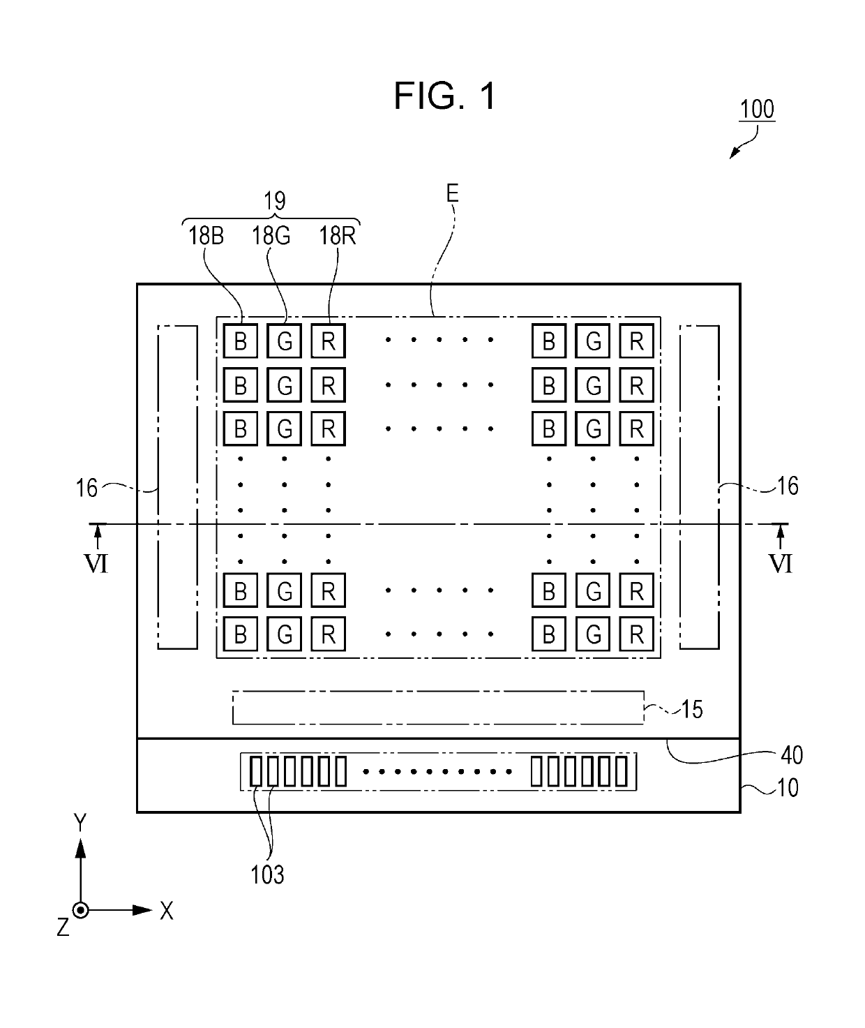
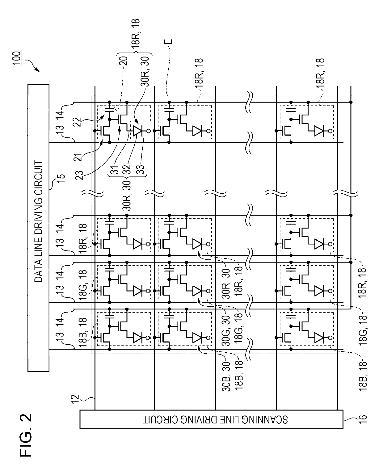
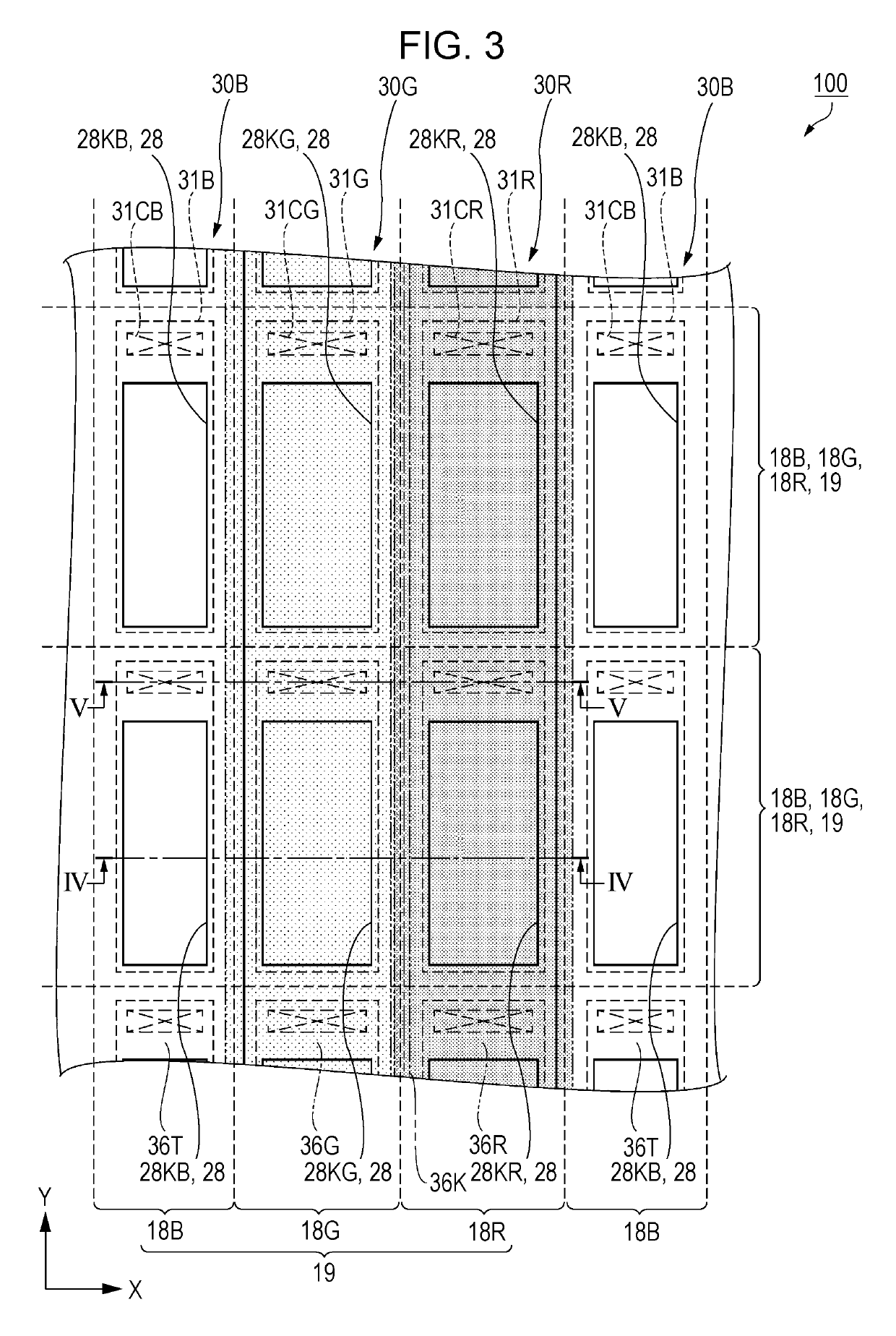
[0067]First, the organic EL device of the embodiment will be described with reference to FIG. 1 to FIG. 5. FIG. 1 is a schematic plan view illustrating a configuration of an organic EL device of a first embodiment, FIG. 2 is an equivalent circuit diagram illustrating an electrical configuration of the organic EL device, and FIG. 3 is a schematic plan view illustrating disposition of organic EL elements and color filters in a sub-pixel of the organic EL device. FIG. 4 is a sectional view schematically illustrating a structure of the sub-pixel taken along line IV-IV in FIG. 3, and FIG. 5 is a sectional view schematically illustrating a structure of a contact portion of a pixel electrode in the sub-pixel taken along line V-V in FIG. 3.

[0068]The organic EL device 100 according to the embodiment is a white light emitting-type microdisplay which is preferable as a display portion of a head-mounted display (HMD) described below.

[0069]As illustrated in FIG. 1, an organic EL...

second embodiment

Organic EL Device and Method of Manufacturing the Same

[0165]Next, the organic EL device of the second embodiment will be described with reference to FIG. 17 to FIG. 19. FIG. 17 is a schematic plan view illustrating disposition of pixel electrodes and color filters in the organic EL device of the second embodiment, FIG. 18 is a sectional view schematically illustrating a structure of the sub-pixel taken along line XVIII-XVIII in FIG. 17, and FIG. 19 is a sectional view schematically illustrating a structure of a contact portion in a sub-pixel taken along line XIX-XIX in FIG. 17. An organic EL device 200 of the second embodiment is obtained by differentiating the configuration of, particularly, the color filter 36 in the sub-pixel 18 of the organic EL device 100 of the above-described first embodiment, and the same components as those in the organic EL device 100 are denoted by the same reference numerals and the detailed description thereof will be omitted.

[0166]As illustrated in FIG...

third embodiment

Organic EL Device and Method of Manufacturing the Same

[0181]Next, the organic EL device of the third embodiment will be described with reference to FIG. 20 and FIG. 21. FIG. 20 is a schematic plan view illustrating disposition of pixel electrodes and color filters in the organic EL device of the third embodiment, and FIG. 21 is a sectional view schematically illustrating a structure of the sub-pixel taken along line XXI-XXI in FIG. 20. An organic EL device 300 of the third embodiment is obtained by differentiating the configuration of, particularly, the color filter 36 in the sub-pixel 18 of the organic EL device 100 of the above-described first embodiment, and the same components as those in the organic EL device 100 are denoted by the same reference numerals and the detailed description thereof will be omitted.

[0182]As illustrated in FIG. 20, the organic EL device 300 of the embodiment includes the plurality of sub-pixels 18 which are arranged in a matrix shape in the X direction ...


PUM


Abstract

Provided is an organic EL device including a first substrate, a first organic EL element and a second organic EL element which is provided on the first substrate, a sealing layer which covers the first organic EL element and the second organic EL element, and a color filter which is provided on the sealing layer. The color filter includes a coloring layer overlapping the first organic EL element in a planar view, and a resin layer overlapping the second organic EL element in a planar view.

Description

BACKGROUND[0001]1. Technical Field[0002]The present invention relates to an organic EL device which is provided with an electro-luminescence (EL) element, a method of manufacturing the organic EL device, and an electronic device which is provided with the organic EL device.[0003]2. Related Art[0004]Since the organic EL element can be easily miniaturized and thinned as compared with a light emitting diode (LED), the organic EL element being applied to a microdisplay such as a head-mounted display (HMD) and an electronic viewer (EVF), as a light-emitting element has attracted attention.[0005]As means for realizing a color display in such a microdisplay, a configuration of combining an organic EL element which can emit white light with a color filter is considered. When the light emitted from the organic EL element is incident on a predetermined coloring layer in the color filter, it is possible to realize excellent display quality, and thus arranging the coloring layers in a position ...

Claims


Application Information

Patent Timeline
Patent Type & Authority Patents(United States)
IPC IPC(8): H01L27/32H01L51/52H01L51/56H01L27/12
CPCH01L27/3248H01L27/322H01L27/3206H01L51/5206H01L51/5221H01L51/5265H01L51/56H01L27/1214H01L27/3211H01L27/3216H01L27/3262H01L51/5246H01L51/5253H01L51/5271H01L2227/323H01L2251/5315H01L2251/558H05B33/22H10K59/38H10K59/876H10K59/8731H10K59/878H10K59/30H10K59/352H10K59/123H10K59/1213H10K2102/3026H10K2102/351H10K50/81H10K50/82H10K50/852H10K71/00H10K50/844H10K50/856H10K50/8426H10K59/35H10K59/1201
Inventor HANAMURA, YUKISHIRATORI, KOYAKOSHIHARA, TAKESHI
Owner SEIKO EPSON CORP
Learn More