Electrooptical device, electronic apparatus, and head mount display

a technology of electronic equipment and display screen, applied in static indicating devices, instruments, optical elements, etc., can solve problems such as color deviation caused by viewing angle, and achieve the effects of reducing discomfort, excellent visibility, and reducing color deviation

Active Publication Date: 2019-07-30
LUMITEK DISPLAY TECH LTD
View PDF16 Cites 2 Cited by
  • Summary
  • Abstract
  • Description
  • Claims
  • Application Information

AI Technical Summary

Benefits of technology

[0009]In this configuration of this application example, a length of a region between the first sub-pixel and the second sub-pixel with different colors in the first direction is the same as a length of a region between the third sub-pixel and the fourth sub-pixel with different colors in the first direction. Thus, it is possible to reduce a difference in a color mixing state of the region between the sub-pixels with different colors, the difference being caused by viewing angle in the first direction. That is, it is possible to provide the electrooptical device capable of reducing color deviation which is caused by the viewing angle in the first direction. In addition, the region between the sub-pixels in the first direction is set as the pixel contact region, and the sub-pixels with different colors are partitioned by the pixel contact region. Thus, it is possible to realize an electrical connection between the sub-pixels with different colors. In other words, there is no need to provide a dedicated configuration for partition of the sub-pixels with different colors in the first direction.
[0041]In this application example, it is possible to provide the head mount display capable of reducing the color deviation which is caused by the viewing angle in at least the first direction and configured such that display can be recognized with excellent visibility. In particular, by applying the electrooptical device according to the application example for both eyes, it is possible to reduce discomfort due to the color deviation of an image recognized by both eyes, and thus it is possible to provide the head mount display with little fatigue in image recognition even when used for longer periods of time.

Problems solved by technology

When such a color mixing state is referred to as color deviation which is caused by viewing angle, there is a problem that color deviation which is caused by viewing angle occurs.

Method used


Image

  • Electrooptical device, electronic apparatus, and head mount display
  • Electrooptical device, electronic apparatus, and head mount display
  • Electrooptical device, electronic apparatus, and head mount display

Examples


first embodiment

Electrooptical Device

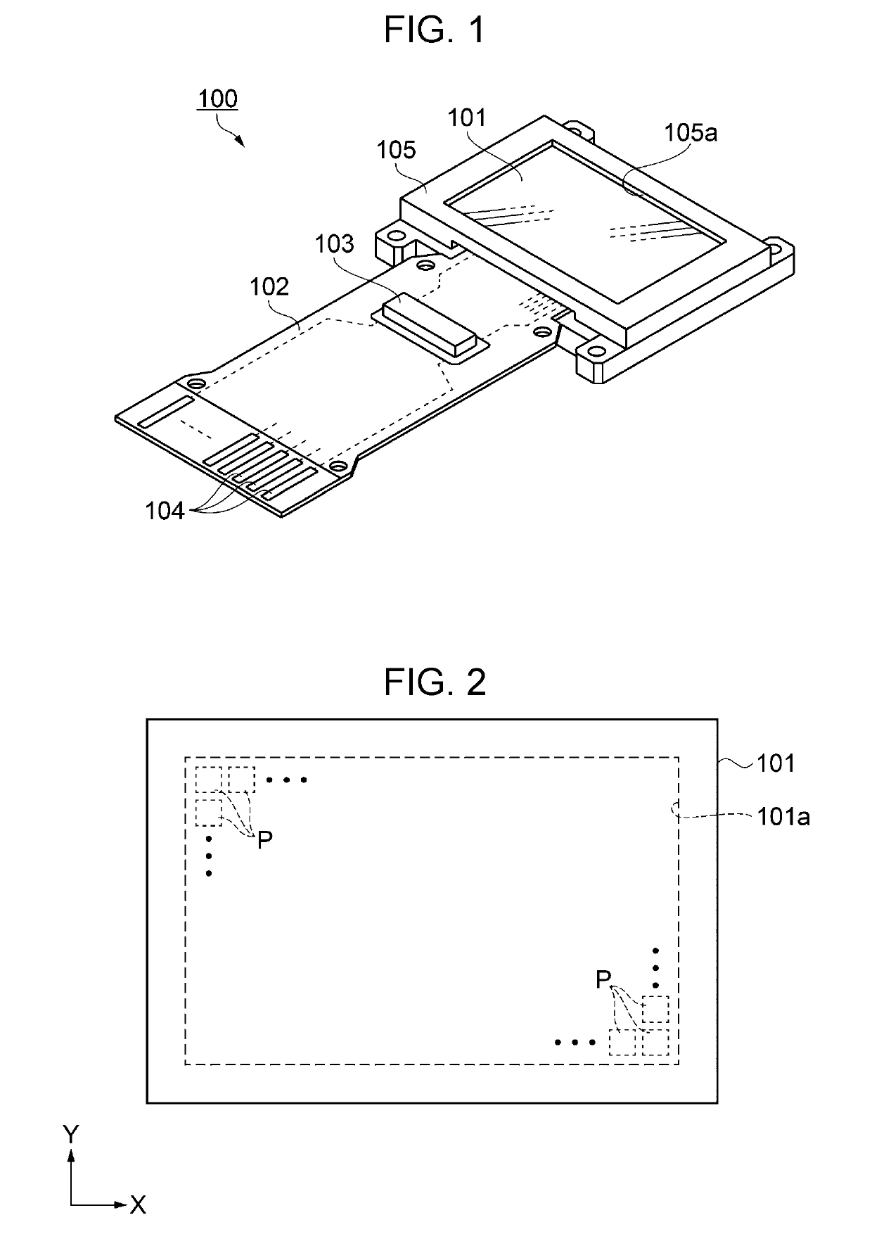
[0071]First, a basic configuration example of an electrooptical device according to the present embodiment will be described with reference to FIGS. 1 and 2. FIG. 1 is a perspective view illustrating a configuration of the electrooptical device, and FIG. 2 is a schematic plan view illustrating an arrangement of display units (pixels) of a display panel.

[0072]The electrooptical device 100 according to the present embodiment is a display device capable of color display, and includes a display panel 101, a flexible printed circuit board 102 on which a driver IC 103 for driving the display panel 101 is mounted (hereinafter, referred to as an FPC 102), and a frame body 105 for housing the display panel 101 and fixing the display panel 101 to a support base or the like.

[0073]The FPC 102 is electrically connected to the display panel 101, and includes a plurality of external connection terminals 104 for inputting input signals such as image information to the driver IC...

second embodiment

[0158]FIG. 14 is a schematic plan view illustrating an arrangement of the sub-pixels and the pixel contact regions in the electrooptical device according to a second embodiment.

[0159]As illustrated in FIG. 14, in the second embodiment, in the pixel P1 and the pixel P2 adjacent to each other in the X direction, the arrangement in the X direction of the sub-pixel 110G and the sub-pixel 110R is made different from that of the first embodiment. More specifically, the sub-pixel 110G, the pixel contact region CH10, the sub-pixel 110R, the pixel contact region CH9, the sub-pixel 110R, the pixel contact region CH9, the sub-pixel 110G, and the pixel contact region CH10 are disposed in the X direction in this order. The sub-pixels 110R with the same color are disposed in the X direction with the pixel contact region CH9 interposed therebetween, and the sub-pixels 110G with the same color are disposed in the X direction with the pixel contact region CH10 interposed therebetween. In the pixel P...

third embodiment

[0165]FIG. 15 is a schematic plan view illustrating an arrangement of the sub-pixels and the pixel contact regions in the electrooptical device according to a third embodiment.

[0166]As illustrated in FIG. 15, the third embodiment is different from the first embodiment in the arrangement of the pixel contact regions. Specifically, the sub-pixel 110G and the sub-pixel 110R are disposed in this order to be parallel to each other with a distance d5 in the X direction. The sub-pixel 110B is repeatedly disposed with a distance d7 in the X direction. Each of the sub-pixels 110B, 110G, and 110R illustrated in FIG. 15 indicates each of the light emitting regions thereof.

[0167]The light emitting regions of the sub-pixel 110G and the sub-pixel 110R have a width d1 in the X direction, and the light emitting region of the sub-pixel 110B has a width d3 in the X direction that is wider than the width d1. The light emitting regions of the sub-pixel 110G and the sub-pixel 110R have a width d2 in the...


PUM


Abstract

An electrooptical device includes a first sub-pixel, a first region, a second sub-pixel, a second region, a third sub-pixel, a third region, a fourth sub-pixel, and a fourth region, which are arranged in an X direction as a first direction. The first sub-pixel and the second sub-pixel have different colors from each other, the third sub-pixel and the fourth sub-pixel have different colors from each other, and the first region, the second region, the third region, and the fourth region have the same length in the X direction.

Description

BACKGROUND1. Technical Field[0001]The present invention relates to an electrooptical device, an electronic apparatus, and a head mount display.2. Related Art[0002]As an electrooptical device, for example, a display device has been proposed (JP-A-2009-282190). In the display device, light emitting elements with a plurality of colors are formed on a substrate for each pixel, the light emitting elements including a light emitting element which emits blue light, a plurality of pixels are disposed in a matrix, the pixel being configured in units of sub-pixels with a plurality of colors, and a relative position relationship between transistors of each sub-pixel with each emission color and a light emitting portion of the light emitting element which emits blue light is laid out such that distances between the transistors of each sub-pixel and the light emitting portion are the same for each color.[0003]According to the display device described in JP-A-2009-282190, even when a part of blue...

Claims


Application Information

Patent Timeline
Patent Type & Authority Patents(United States)
IPC IPC(8): H01L27/32G02B27/01H01L51/52
CPCH01L27/3211G02B27/0172H01L27/3218H01L27/3248H01L51/5203H01L27/3276H01L2251/5315G02B2027/0112H01L27/3213H01L27/3216G09G3/2003G09G3/2074G09G3/3233G09G3/3266G09G2320/0626G09G2320/045G09G2320/043G09G2310/0289G09G2320/0233G09G2300/0842G09G2300/0852G09G2300/0819G09G2300/0452G09G2300/0443H10K59/351H10K59/35H10K59/352H10K59/353H10K59/12H10K59/121H10K59/1213H10K59/1216H10K59/131H10K59/123H10K2102/3026H10K50/805
Inventor OTA, HITOSHIKOSHIHARA, TAKESHI
Owner LUMITEK DISPLAY TECH LTD
Why Eureka
Try Eureka