Fin and shallow trench isolation replacement to prevent gate collapse

a technology of shallow trenches and gate collapse, applied in the direction of semiconductor devices, electrical equipment, transistors, etc., can solve the problems of high aspect ratio gates, severe undercutting, poor quality materials,

Inactive Publication Date: 2019-08-06
INT BUSINESS MASCH CORP
View PDF15 Cites 0 Cited by
  • Summary
  • Abstract
  • Description
  • Claims
  • Application Information

AI Technical Summary

Problems solved by technology

Flowable oxide is generally a poor quality material and causes severe undercutting in the STI areas during CMOS dual epitaxy processes.
The undercutting typically causes high aspect ratio gates to collapse.

Method used


Image

  • Fin and shallow trench isolation replacement to prevent gate collapse
  • Fin and shallow trench isolation replacement to prevent gate collapse
  • Fin and shallow trench isolation replacement to prevent gate collapse

Examples


Embodiment Construction

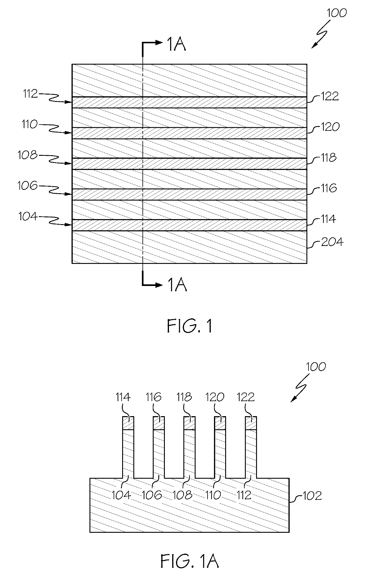
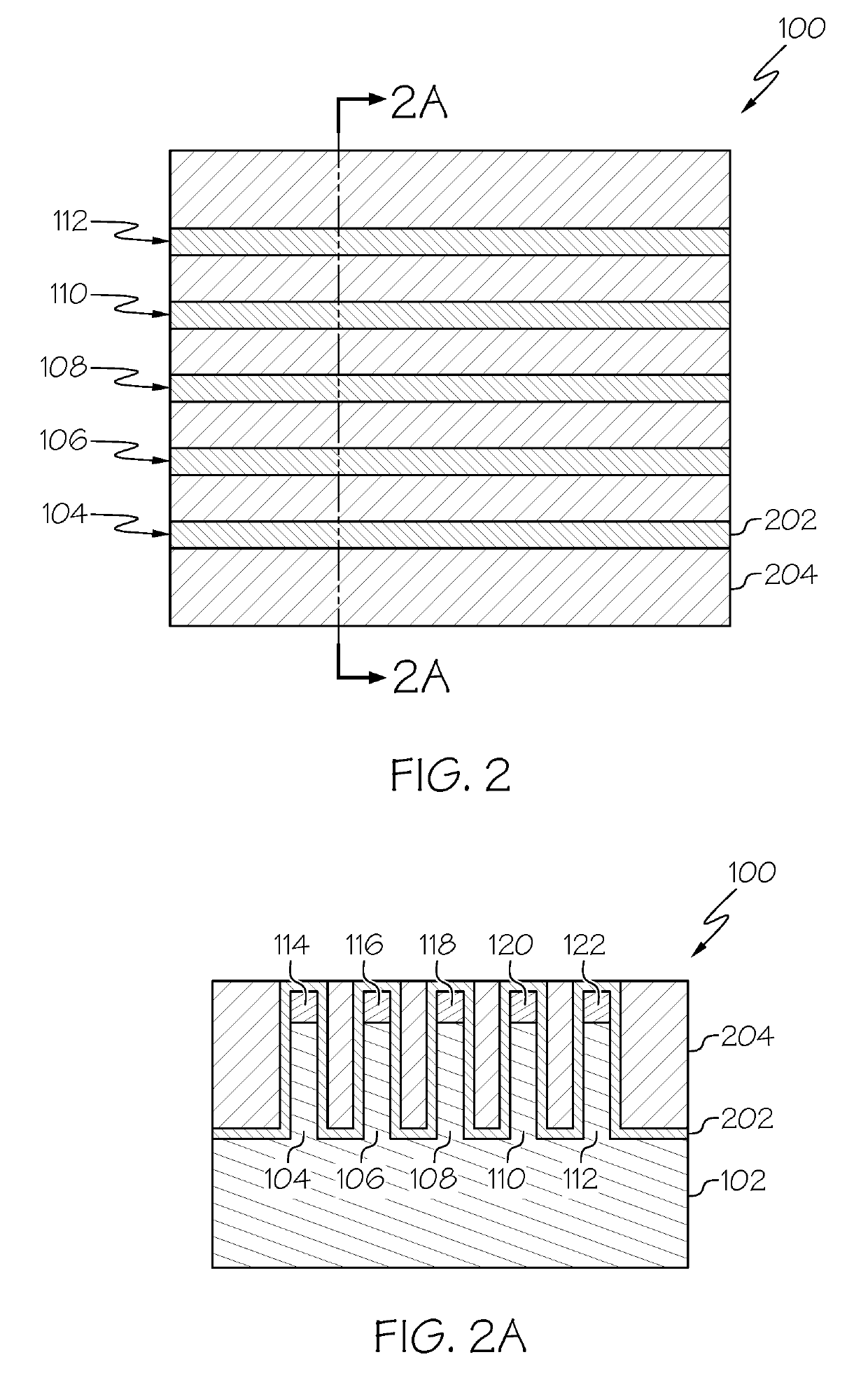
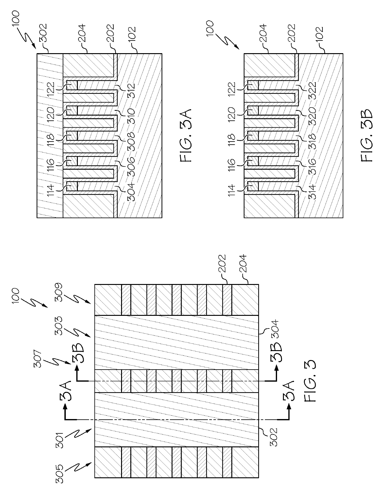
[0026]It is to be understood that the present disclosure will be described in terms of a given illustrative architecture; however, other architectures, structures, substrate materials and process features and steps may be varied within the scope of the present disclosure.

[0027]It will also be understood that when an element such as a layer, region or substrate is referred to as being “on” or “over” another element, it can be directly on the other element or intervening elements may also be present. In contrast, when an element is referred to as being “directly on” or “directly over” another element, there are no intervening elements present. It will also be understood that when an element is referred to as being “connected” or “coupled” to another element, it can be directly connected or coupled to the other element or intervening elements may be present. In contrast, when an element is referred to as being “directly connected” or “directly coupled” to another element, there are no ...


PUM


Abstract

A semiconductor structure and a method for fabricating the same. The structure includes a substrate, active fin structures, and non-active fin structures. The structure further includes isolation regions in contact with the active fin structures, and isolation regions in contact with the non-active fin structures. A first gate structure is in contact with the active fin structures and the isolation regions that are in contact with the active fin structures. A second gate structure is in contact with the non-active fin structures. The method includes forming an isolation region between fin structures. A mask is formed over active fin structures and dummy fin structures are then removed to form a plurality of trenches between the isolation regions. A nitride-based layer is formed in contact with isolation regions corresponding to the dummy fin structures. The nitride-based layer forms a non-active fin structure within each trench of the trenches.

Description

BACKGROUND[0001]The present invention generally relates to semiconductor devices, and more particularly relates to preventing gate collapse during fabrication of semiconductor devices.[0002]In many instances, fabrication processes for fin field-effect-transistors (finFETs) utilize flowable oxide in the shallow trench isolation (STI) area to ensure STI oxide gap fill. Flowable oxide is generally a poor quality material and causes severe undercutting in the STI areas during CMOS dual epitaxy processes. The undercutting typically causes high aspect ratio gates to collapse.SUMMARY OF THE INVENTION[0003]In one embodiment, a method for forming a semiconductor structure is provided. The method comprises forming an isolation region between each fin structure of a plurality of fin structures. Each isolation region comprises an isolation material. A mask is formed over active fin structures of the plurality of fin structures. Dummy fin structures of the plurality of fin structures remain expo...

Claims


Application Information

Patent Timeline
Patent Type & Authority Patents(United States)
IPC IPC(8): H01L29/66H01L21/8234H01L27/088H01L29/06
CPCH01L29/6681H01L21/823431H01L29/0653H01L27/0886H01L21/823481
Inventor SEO, SOON-CHEON
Owner INT BUSINESS MASCH CORP
Why Eureka
Try Eureka