Semiconductor memory device

a memory device and semiconductor technology, applied in the field of semiconductor memory devices, can solve the problems of long precharge time and large precharge current, and achieve the effect of reducing the precharge tim

Active Publication Date: 2019-09-17
SAMSUNG ELECTRONICS CO LTD
View PDF10 Cites 2 Cited by
  • Summary
  • Abstract
  • Description
  • Claims
  • Application Information

AI Technical Summary

Benefits of technology

[0005]Aspects of the inventive concept provide a semiconductor memory device which can reduce a precharge time by precharging a bit line of a memory cell array using a current according to an operating temperature.

Problems solved by technology

When an operating temperature of the semiconductor memory device is high, the precharge time may be long due to a leakage current or the like.
Therefore, when the operating temperature of the semiconductor memory device is high, a relatively large precharge current may be required.
On the other hand, when the operating temperature of the semiconductor memory device is low, if the bit line is precharged using a relatively large precharge current as in the case where the operating temperature of the semiconductor memory device is high, it may be over-precharged.

Method used


Image

  • Semiconductor memory device
  • Semiconductor memory device
  • Semiconductor memory device

Examples


Embodiment Construction

[0019]It will be understood that, although the terms first, second, third etc. may be used herein to describe various elements, these elements should not be limited by these terms. Unless indicated otherwise, these terms are generally used to distinguish one element from another. Thus, a first element discussed below in one section of the specification could be termed a second element in a different section of the specification without departing from the teachings of the present disclosure. Also, terms such as “first” and “second” may be used in the claims to name an element of the claim, even thought that particular name is not used to describe in connection with the element in the specification.

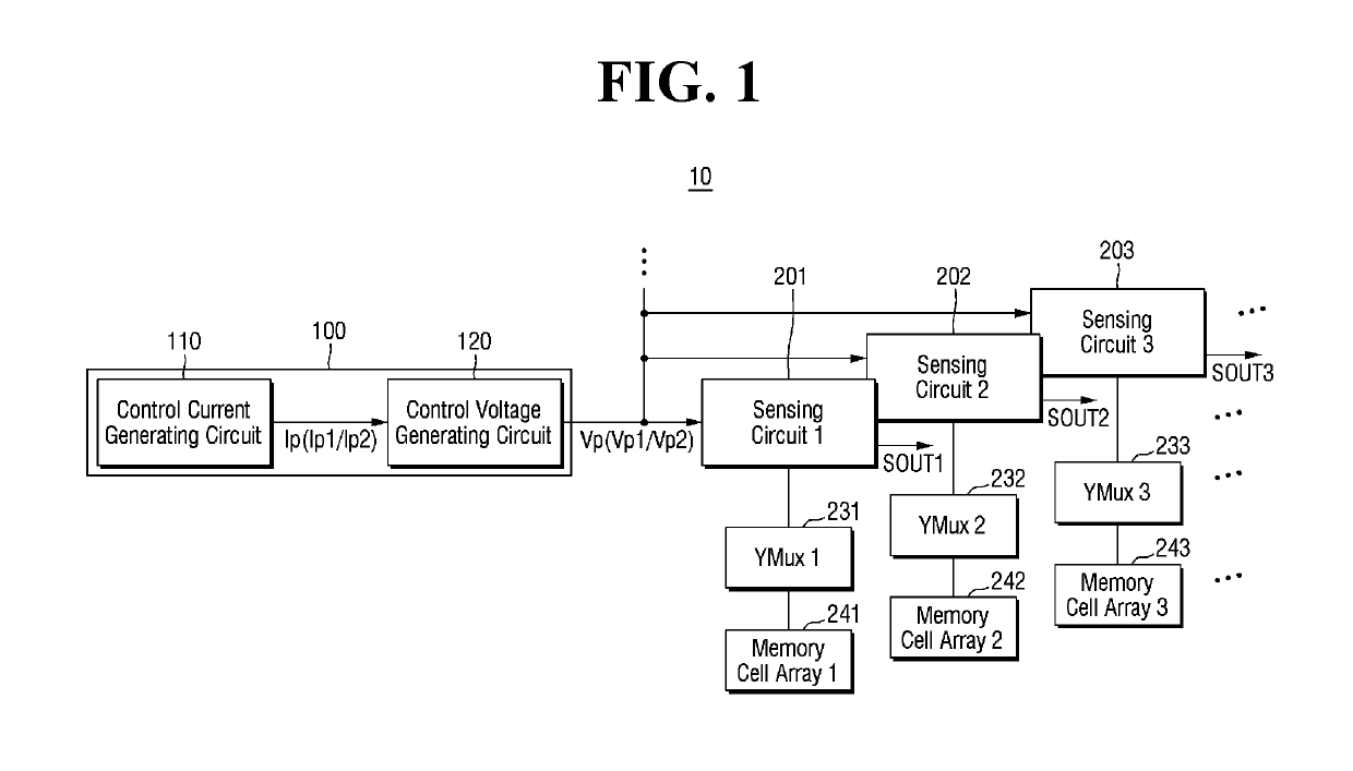
[0020]FIG. 1 is a block diagram of a semiconductor memory device 10 according to example embodiments.

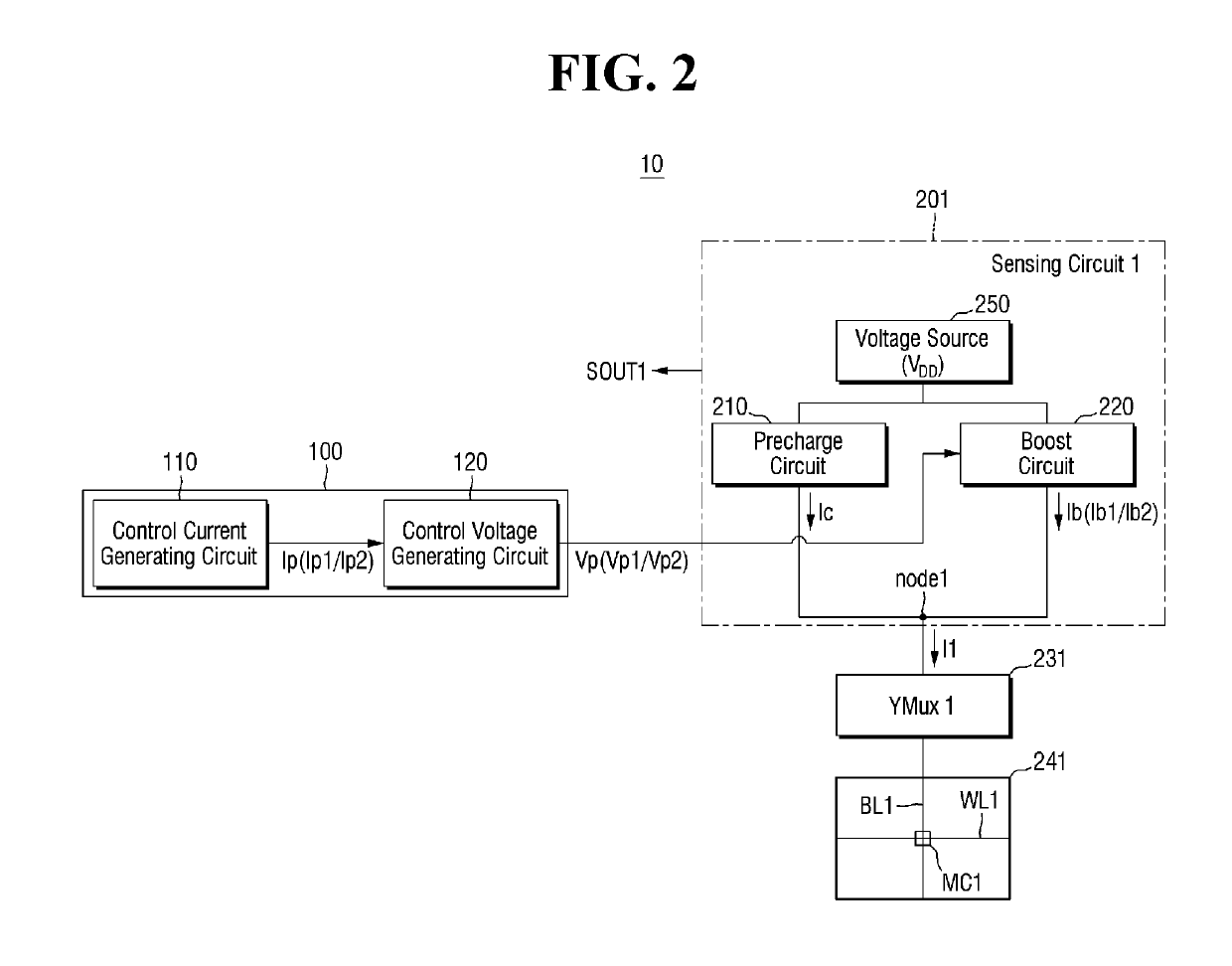
[0021]Referring to FIG. 1, the semiconductor memory device 10 may include a control signal generating circuit 100, a first sensing circuit 201, a second sensing circuit 202, a third sensing ...


PUM


Abstract

A semiconductor memory device includes a memory cell array including a plurality of memory cells connected to a plurality of bit lines, a control signal generating circuit configured to generate a first control signal in response to a first operating temperature of the semiconductor memory device and a second control signal in response to a second operating temperature of the semiconductor memory device, a precharge circuit configured to provide a precharge current to a first bit line of the plurality of bit lines in response to an enable signal, and a boost circuit configured to provide a boost current to the first bit line in response to the enable signal, wherein the magnitude of the boost circuit is responsive to one of the first and second control signals.

Description

[0001]This application claims the benefit of Korean Patent Application No. 10-2017-0137566, filed on Oct. 23, 2017, in the Korean Intellectual Property Office, the disclosure of which is incorporated herein in its entirety by reference.BACKGROUND1. Field[0002]The present disclosure relates to a semiconductor memory device.2. Description of the Related Art[0003]To sense an on / off memory cell in a nonvolatile memory device, an on current flowing through a bit line of a memory cell array may be used. The bit line of the memory cell array may be precharged to allow the on current to flow through the bit line. For accurate on / off memory cell sensing, the bit line of the memory cell array may be precharged to a certain level.[0004]When an operating temperature of the semiconductor memory device is high, the precharge time may be long due to a leakage current or the like. Therefore, when the operating temperature of the semiconductor memory device is high, a relatively large precharge curr...

Claims


Application Information

Patent Timeline
Patent Type & Authority Patents(United States)
IPC IPC(8): G11C7/12G11C16/24G11C16/34G11C16/30G11C5/14G11C7/08G11C7/06G11C16/26G11C7/04G11C16/04
CPCG11C5/145G11C16/26G11C16/24G11C7/062G11C16/3418G11C7/04G11C16/30G11C7/08G11C16/0425G11C7/067G11C7/12
Inventor SHIN, HYUN-JIN
Owner SAMSUNG ELECTRONICS CO LTD
Why Eureka
Try Eureka