Memory and Sense Amplifiers
A technology for sensitive amplifiers and control terminals, applied in the field of memory and sensitive amplifiers, can solve the problems of unreadable and slowed memory reading speed, and achieve the effects of reducing pre-charging time, increasing reading speed, and enhancing channel conductivity
- Summary
- Abstract
- Description
- Claims
- Application Information
AI Technical Summary
Problems solved by technology
Method used
Image
Examples
Embodiment 1
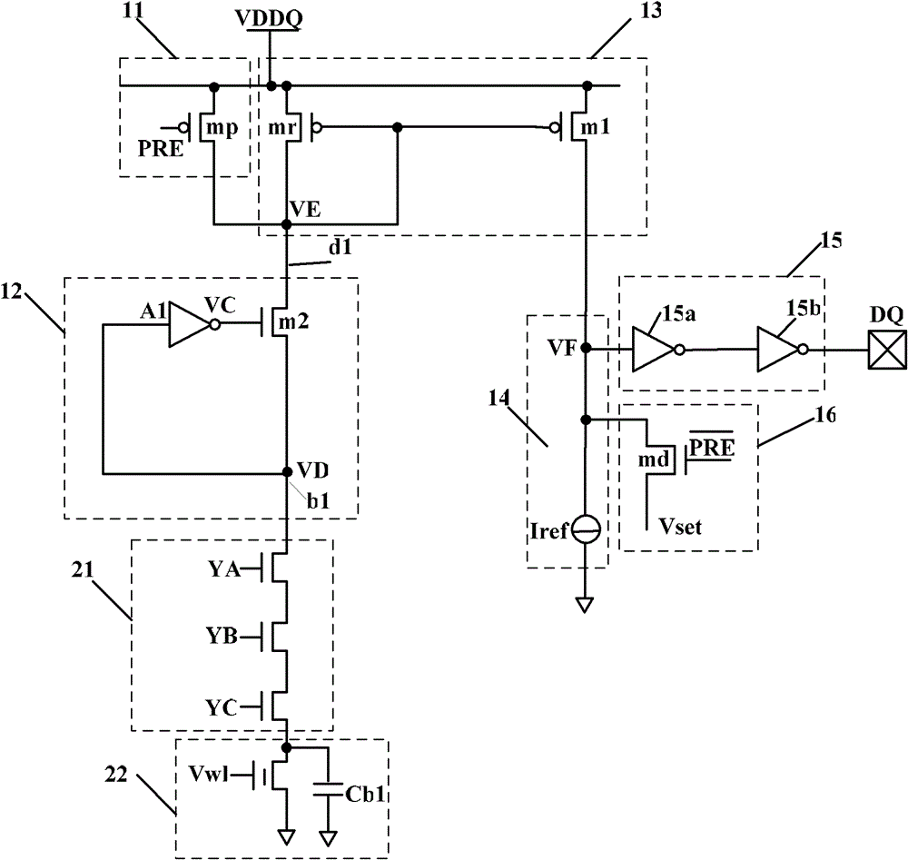
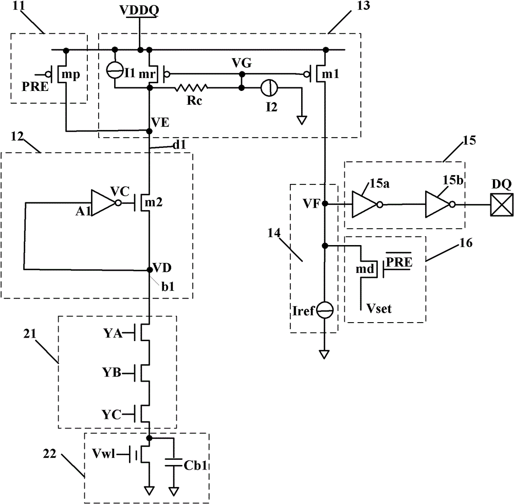
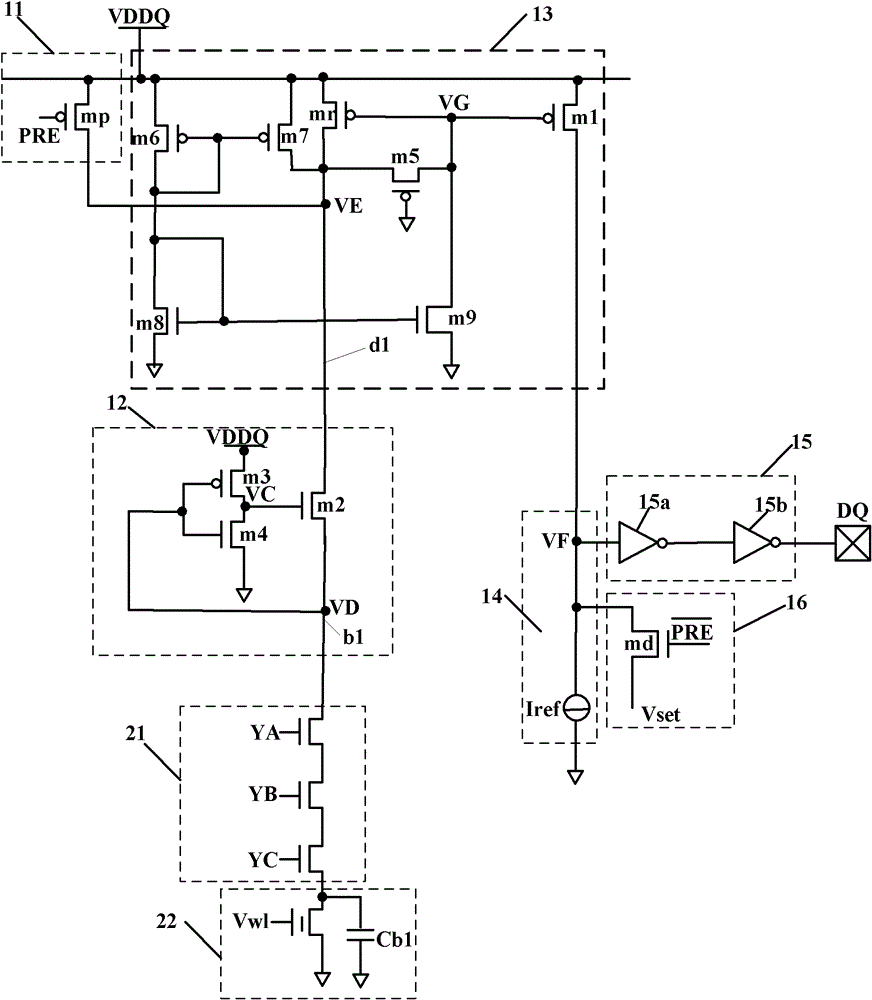
[0047] see image 3 As shown, the sense amplifier provided in this embodiment includes: a precharge unit 11 , a bit line adjustment unit 12 , a current mirror unit 13 , a comparison unit 14 , a bias unit 16 and an output unit 15 .
[0048] The pre-charging unit 11 charges the data line d1 when the bit line is pre-charged (before reading the memory cell), that is, increases the voltage of the data line node VE (data line voltage).
[0049] The pre-charging unit 11 includes a pre-charging transistor m P , precharge transistor m P The gate is input with the precharge control signal PRE, the source is input with the working voltage source VDDQ, and the drain is connected to the data line node VE (or in other words, connected to the data line dl), that is, the output data line voltage.
[0050] The bit line adjustment unit 12, when the bit line is precharged, feeds back and amplifies the voltage of the bit line node VD (bit line voltage) to obtain a feedback voltage. Under the co...
Embodiment 2
[0064] see Figure 4 As shown, the structure of the sense amplifier provided in this embodiment is substantially the same as that of the sense amplifier in Embodiment 1, and the difference is that the bit line adjustment unit 12 includes: a regulated power supply Vreg, a feedback transistor m10, an impedance transistor m11 and an adjustment transistor m2. The feedback transistor m10 , the impedance transistor m11 and the adjustment transistor m2 all include a control terminal (gate), a first terminal (source) and a second terminal (drain). The output terminal of the regulated power supply Vreg is connected to the first terminal of the feedback transistor m10, and the regulated power supply Vreg provides the first terminal of the feedback transistor m10 with a value range including: 0.8V~2V working voltage; the second terminal of the feedback transistor m10 Connect the feedback node VC, that is, output the feedback voltage; the control terminal of the feedback transistor m10 i...
PUM
 Abstract
Description
Claims
Application Information


