Full-laser scribing method for large-area copper indium gallium selenide thin-film solar cell module
a solar cell module and copper indium gallium selenide technology, applied in the field of thin-film solar cells, can solve the problems of increasing the manufacturing cost of the module and the high power loss of the module, and achieve the effects of reducing the dead zone area of the module, improving the module power, and increasing the module production efficiency
- Summary
- Abstract
- Description
- Claims
- Application Information
AI Technical Summary
Benefits of technology
Problems solved by technology
Method used
Image
Examples
embodiment 1
[0031
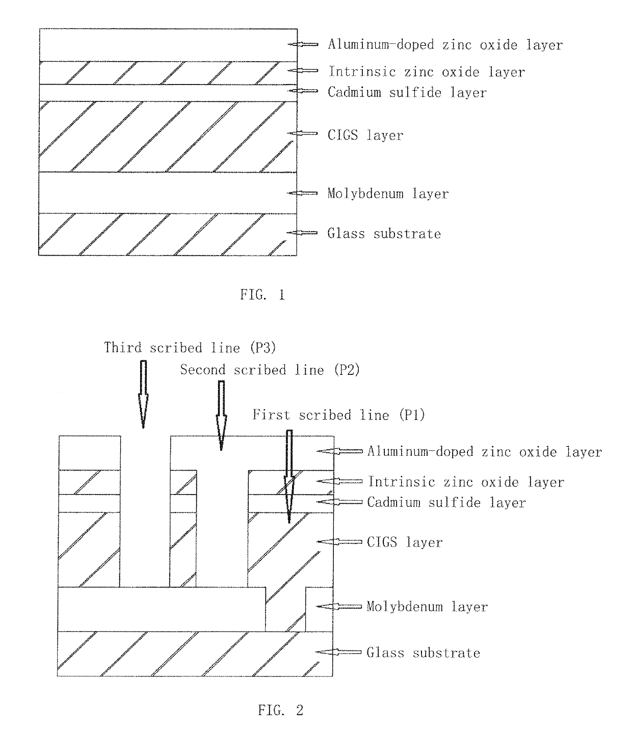
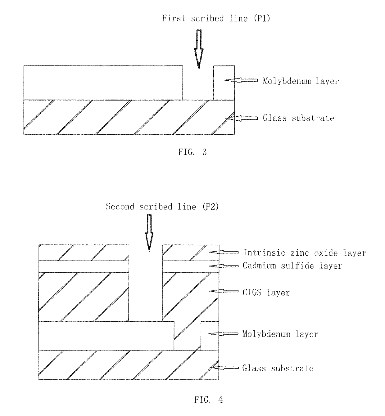
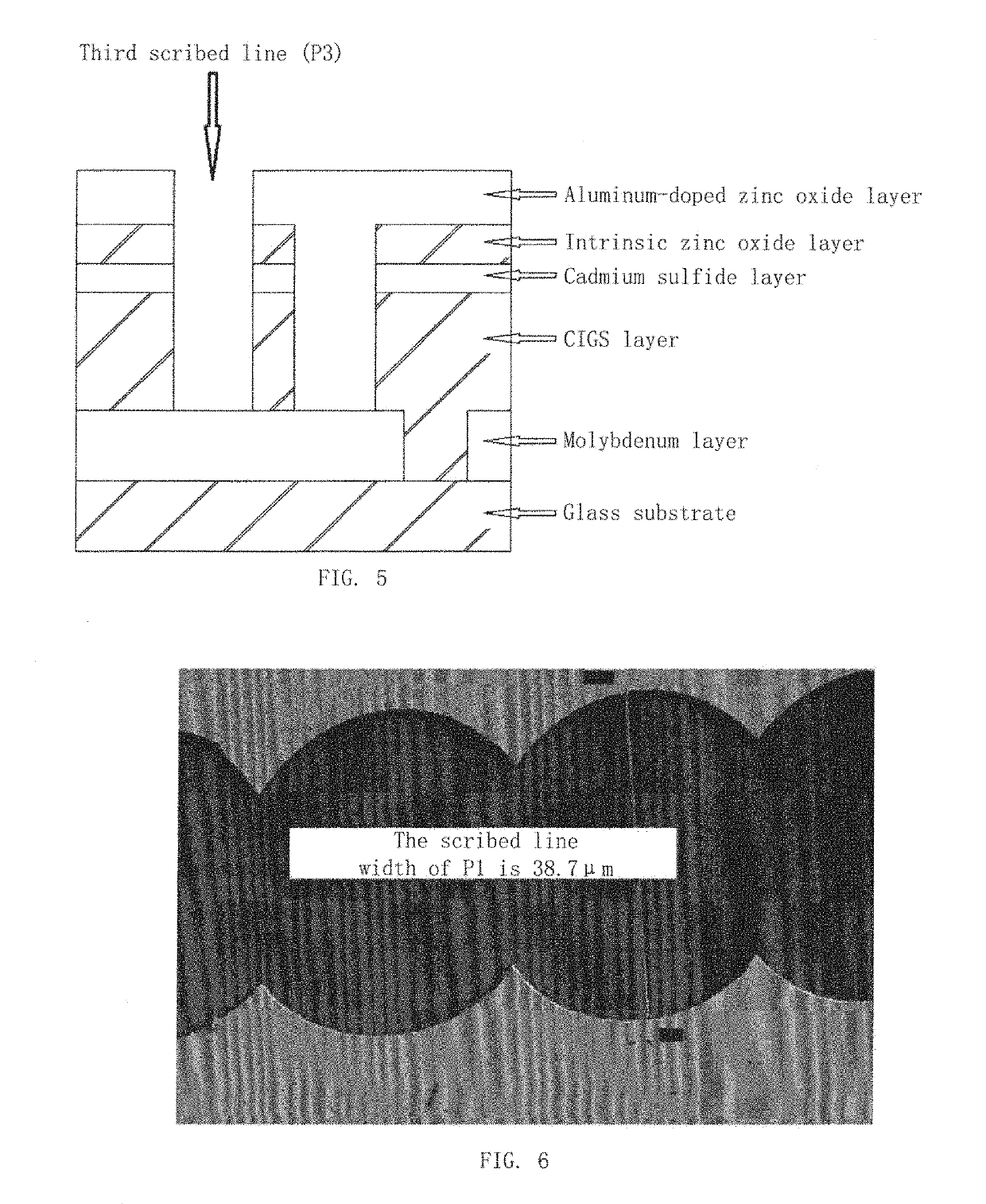
[0032]FIG. 1 is a schematic view of a structure of a large-area copper indium gallium selenide thin-film solar cell according to the present invention. As shown in FIG. 1, the cell includes a glass substrate, a molybdenum layer, a copper indium gallium selenide layer, a cadmium sulfide layer, an intrinsic zinc oxide layer and the aluminum-doped zinc oxide layer. FIG. 2 is a schematic diagram of a full-laser scribing method for a copper indium gallium selenide thin-film solar cell module according to the present invention; as shown in FIG. 2, the full-laser scribing method comprises laser scribing of three scribed lines: first, preparing a molybdenum film on the glass substrate, and using a laser I to scribe off the prepared molybdenum film to form the first scribed line (P1); preparing the following film layers on the molybdenum layer in which P1 has been scribed: a CIGS thin film, a cadmium sulfide thin film and an intrinsic zinc oxide thin film; using a laser II for scribing ...
embodiment 2
[0042
[0043]Step 1 is the same as that in Embodiment 1.
[0044]Step 2, scribing of P1: using a picosecond laser with pulse width of 8 picoseconds, wavelength of 532 nm, scribing power of 2.5 W, single pulse energy of 31.25 μJ, repetition frequency of 80 kHz to scribe P1 in a sample with laser entering from the back of the film-coated substrate at a scribing speed of 2 m / s, wherein the width of the scribed line is 35 μm, and the molybdenum layer in the scribed line is completely removed to expose the surface of the soda-lime glass.
[0045]Step 3 to step 8 are the same as those in Embodiment 1.
embodiment 3
[0046
[0047]Step 1 is the same as that in Embodiment 1.
[0048]Step 2, scribing of P1: using a nanosecond laser with pulse width of 10 nanoseconds, wavelength of 1064 nm, scribing power of 3.2 W, single pulse energy of 40 μJ, repetition frequency of 80 kHz to scribe P1 in a sample with laser entering from the back of the film-coated substrate at a scribing speed of 2 m / s, wherein the width of the scribed line is 33 μm, and the Mo layer in the scribed line is completely removed to expose the surface of the soda-lime glass.
[0049]Step 3 to step 8 are the same as those in Embodiment 1.
PUM
| Property | Measurement | Unit |
|---|---|---|
| width | aaaaa | aaaaa |
| width | aaaaa | aaaaa |
| thickness | aaaaa | aaaaa |
Abstract
Description
Claims
Application Information


