Full-laser scribing method for flexible stainless steel substrate solar cell module
a solar cell module and stainless steel substrate technology, applied in the field of thin film solar cells, can solve the problems of poor process reproducibility, high module efficiency loss, complex screen printing process, etc., and achieve the effect of reducing production and maintenance costs, reducing the dead zone area of the module, and increasing the production efficiency of the modul
- Summary
- Abstract
- Description
- Claims
- Application Information
AI Technical Summary
Benefits of technology
Problems solved by technology
Method used
Image
Examples
embodiment 1
[0030
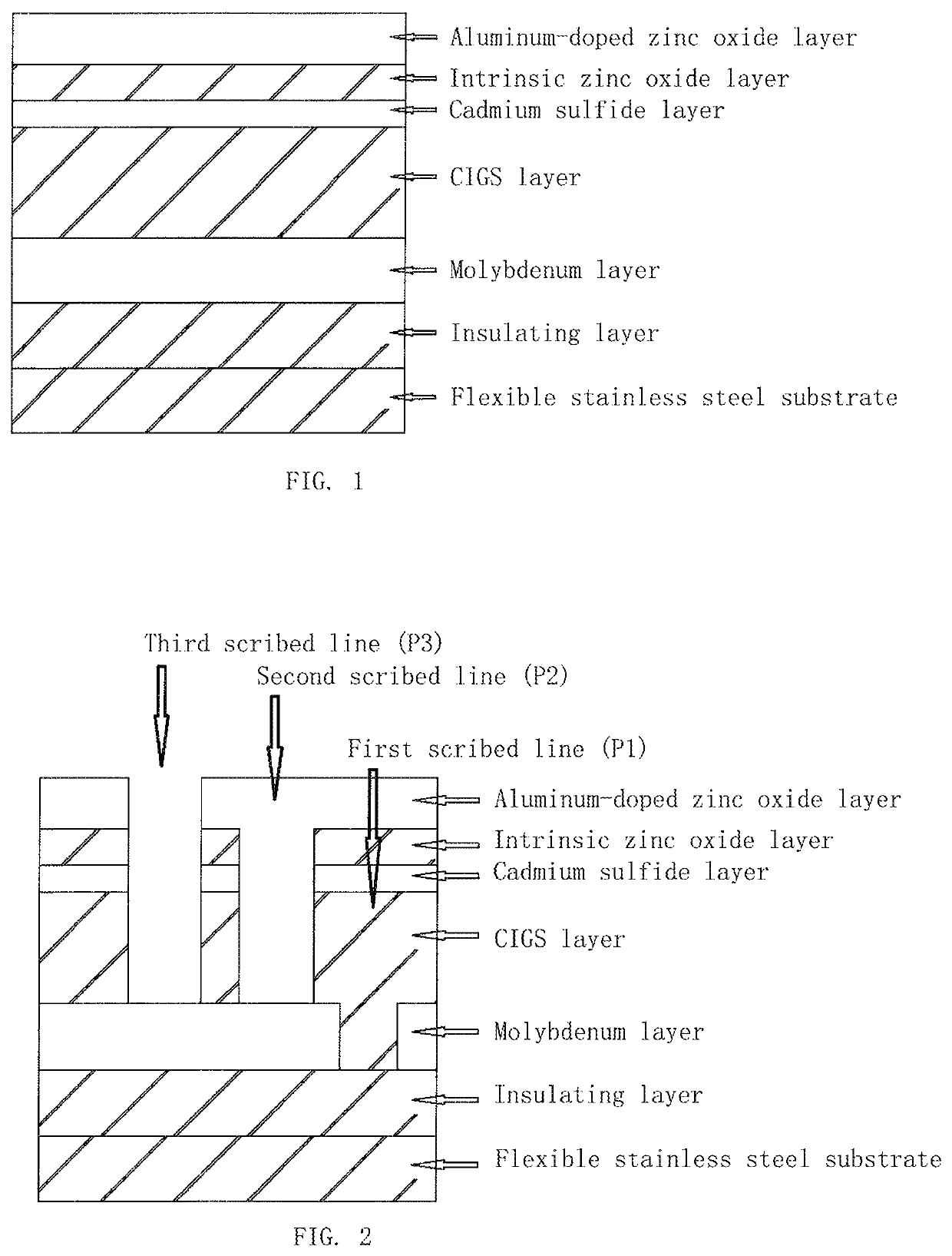
[0031]FIG. 1 shows the structure of the flexible stainless steel substrate CIGS thin-film solar cell according to the present invention. As shown in FIG. 1, the cell includes a stainless steel substrate, an insulating layer, a molybdenum layer, a CIGS layer, a cadmium sulfide layer, an intrinsic zinc oxide layer and an aluminum-doped zinc oxide layer.
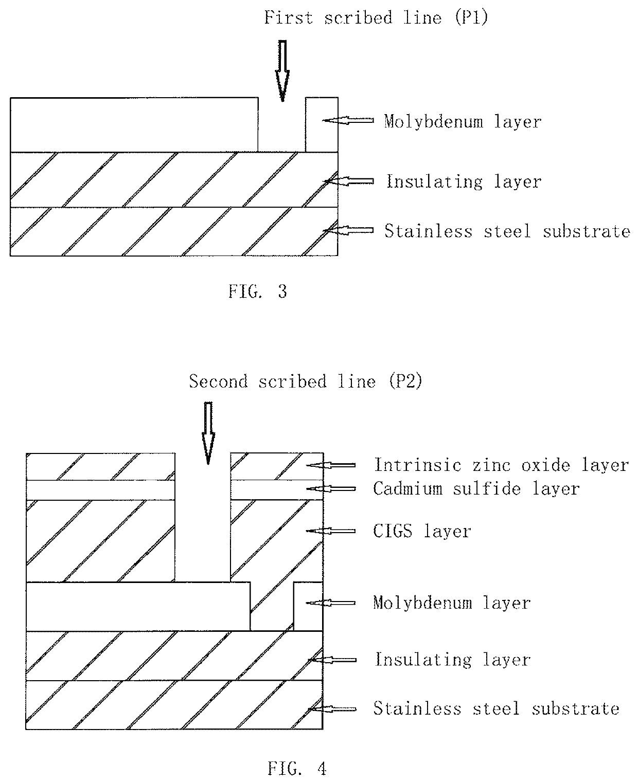
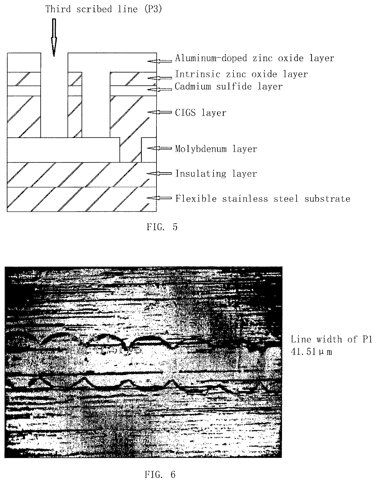
[0032]FIG. 2 shows a full-laser scribing method for the flexible stainless steel substrate CIGS thin-film solar cell according to the present invention. As shown in FIG. 2, the full-laser scribing method comprises laser scribing of three scribed lines: first, preparing an insulating layer and a molybdenum film on a flexible stainless steel substrate, and using a laser I to scribe off the prepared molybdenum film to form a first scribed line (P1), wherein the first scribed line (P1) scribes off the molybdenum layer on the insulating layer without damaging the insulating layer, laser is focused by a focusing lens and then is subjecte...
embodiment 2
[0045
[0046]Step 1: an insulating layer is prepared on a flexible stainless steel substrate in the same way as Embodiment 1.
[0047]Step 2 is the same as that in Embodiment 1.
[0048]Step 3: scribing of P1: a sub-nanosecond laser with pulse width of 800 picoseconds, wavelength of 532 nm, scribing power of 2.7 W, single pulse energy of 33.75 μJ, repetition frequency of 80 kHz is used to scribe P1 in a sample with laser entering from the film-coated surface at a scribing speed of 2 m / s. The width of the scribed line is 40 μm, and the molybdenum layer in the scribed line is completely removed to expose the surface of the insulating layer, without damaging the insulating layer.
[0049]Steps 4-9 are the same as those in Embodiment 1.
embodiment 3
[0050
[0051]Step 1 is the same as that in Embodiment 1.
[0052]Step 2 is the same as that in Embodiment 1.
[0053]Step 3: scribing of P1: a nanosecond laser with pulse width of 100 picoseconds, wavelength of 532 nm, scribing power of 3 W, single pulse energy of 37.5 μJ, repetition frequency of 80 kHz is used to scribe P1 in a sample with laser entering from the film-coated surface at a scribing speed of 2 m / s. The width of the scribed line is 38 μm, and the molybdenum layer in the scribed line is completely removed to expose the surface of the insulating layer, without damaging the insulating layer.
[0054]Steps 4-9 are the same as those in Embodiment 1.
PUM
| Property | Measurement | Unit |
|---|---|---|
| thickness | aaaaa | aaaaa |
| thickness | aaaaa | aaaaa |
| thickness | aaaaa | aaaaa |
Abstract
Description
Claims
Application Information


