Ultra-high coupling factor monolithic transformers for integrated differential radio frequency amplifiers in system-on-chip devices

a radio frequency amplifier and ultra-high coupling factor technology, applied in the direction of transformer/inductance details, fixed transformers or mutual inductances, inductances, etc., can solve the problems of increasing the noise figure of low noise amplifiers, increasing the insertion loss of baluns and transformers, and a proportionate increase in insertion loss, etc., to achieve low noise amplifiers, improve geometries and winding structures, and ultra-high coupling factor

Active Publication Date: 2019-10-08
SKYWORKS SOLUTIONS INC
View PDF11 Cites 2 Cited by
  • Summary
  • Abstract
  • Description
  • Claims
  • Application Information

AI Technical Summary

Benefits of technology

[0012]The present disclosure contemplates improved geometries and winding structures of the balun and transformer with an ultra-high coupling factor. Furthermore, a large inductance in a small geometric area is contemplated, and high-Q inductors, baluns, and transformers with low insertion loss are possible. Front end circuits, that is, the low noise amplifiers, power amplifiers, and RF switches implemented together with the contemplated balun / transformer are understood to exhibit minimal noise figures, and coexist with power amplifiers characterized by low EVM and high efficiency.

Problems solved by technology

One challenge associated with differential power amplifiers and low noise amplifiers is in the design of baluns for differential to single-ended signal lines and regular transformers for differential to differential signal lines, with high coupling factors in a standard CMOS (complementary metal oxide semiconductor) process.
A further challenge relates to the increases in insertion loss of the balun and the transformer at the input of the low noise amplifier or the output of the power amplifier.
As the number of inductive coils in the printed circuit structures increases for the high levels of coupling that are needed, there is understood to be a commensurate increase in insertion loss.
This may result in an increased noise figure of the low noise amplifier, along with a decreased linear output power of the power amplifier.
As a consequence, increased current consumption may follow, as well as decreased gain for the low noise amplifier and / or the power amplifier chain.

Method used


Image

  • Ultra-high coupling factor monolithic transformers for integrated differential radio frequency amplifiers in system-on-chip devices
  • Ultra-high coupling factor monolithic transformers for integrated differential radio frequency amplifiers in system-on-chip devices
  • Ultra-high coupling factor monolithic transformers for integrated differential radio frequency amplifiers in system-on-chip devices

Examples


first embodiment

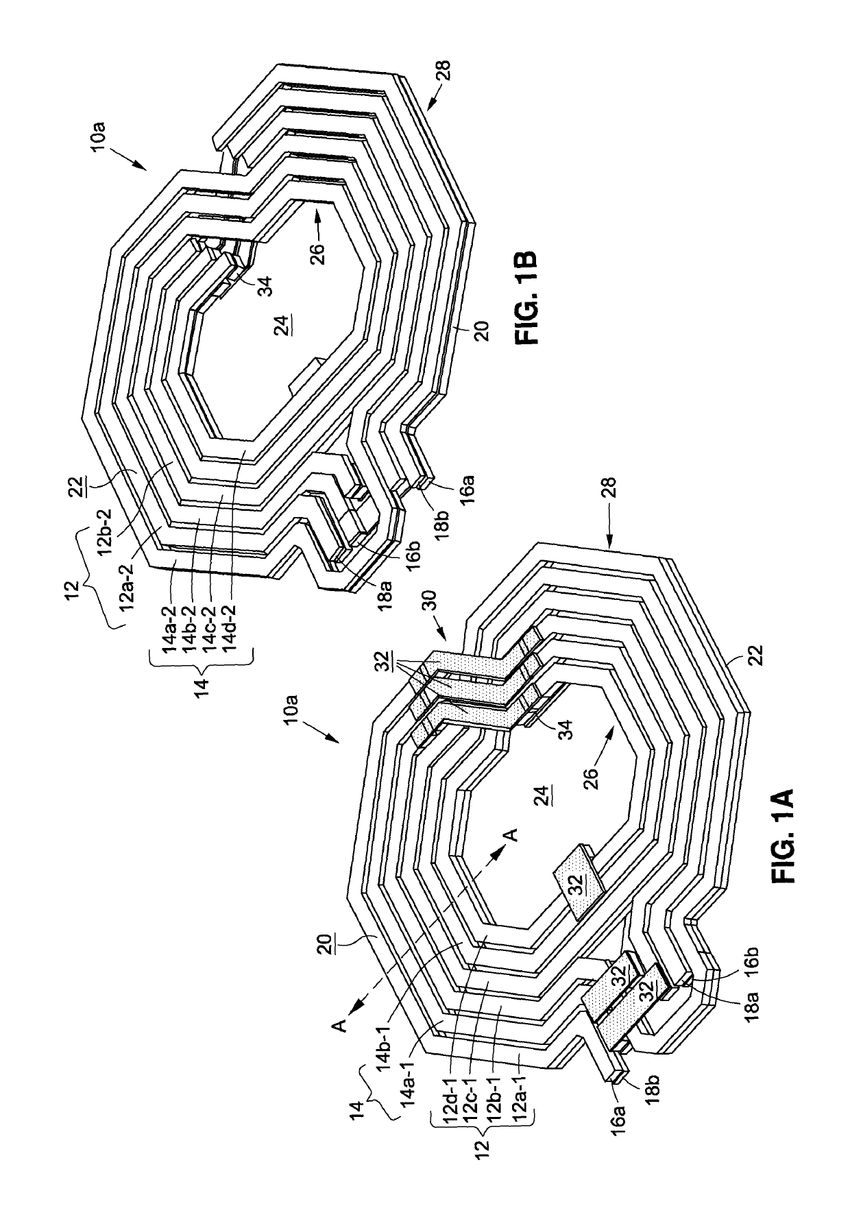
[0046]Referring now to FIGS. 1A and 1B, a transformer 10a includes a primary winding inductor 12 and a secondary winding inductor 14. FIG. 1A depicts a top or first side of the transformer 10a, and FIG. 1B depicts a bottom or second side of the transformer 10a. One end of the primary winding inductor 12 is a first terminal 16a, and on the opposite end of the same is a second terminal 16b. Similarly, one end of the secondary winding inductor 14 is a first terminal 18a. As shown in FIG. 1A, the primary winding inductor 12 is disposed on a first conductive layer 20, though as also shown in FIG. 1B, the primary winding inductor 12 extends to a second conductive layer 22. Moreover, as shown in FIG. 1B, the secondary winding inductor 14 is disposed on the second conductive layer 22, and extends to the first conductive layer 20 as best depicted in FIG. 1A.

[0047]Both the primary winding inductor 12 and the secondary winding inductor 14 are defined by a plurality of turns, and are routed in ...

third embodiment

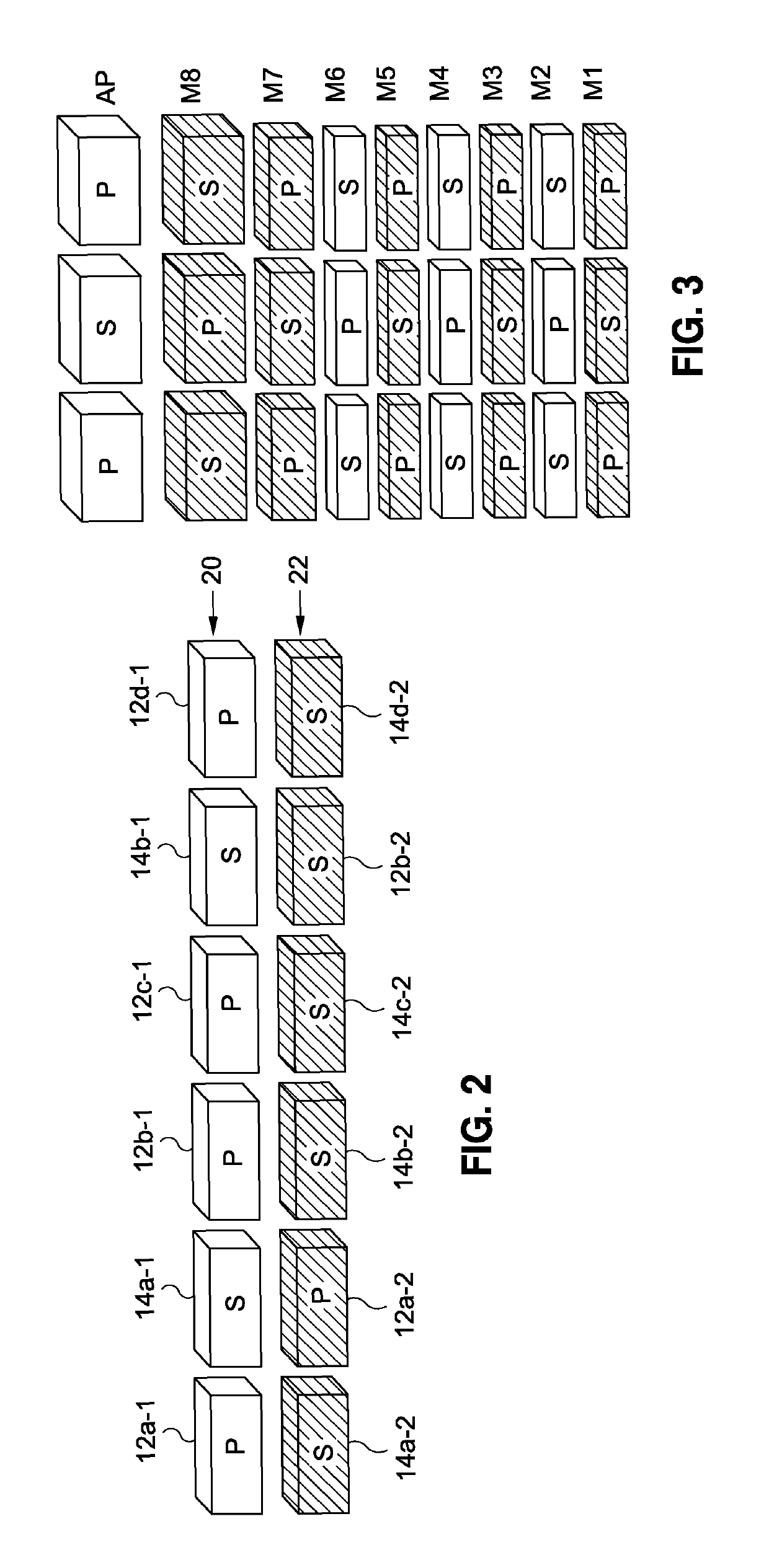
[0067]With specific reference to FIGS. 11A, 12B, and 13, the parts of the primary winding inductor 12 that are on the first conductive layer 20 include a first turn 12a-1, a second turn 12b-1, a third turn 12c-1, and a fourth turn 12d-1. In embodiments utilizing conventional CMOS fabrication processes, the first conductive layer 20 is understood to be the Aluminum layer (AP). The first turn 12a-1 is the outermost portion of the spiral of the primary winding inductor 12, as well as of the overall structure of the transformer 10c.

[0068]Certain segments of the secondary winding inductor 14 are also on the first conductive layer 20. These include a first turn 14a-1, a second turn 14b-1, a third turn 14c-1, a fourth turn 14d-1, and a fifth turn 14e-1. As illustrated, the turns of the primary winding inductor 12 successively alternate with the turns of the secondary winding inductor 14 except for the fifth turn 14e-1, which is adjacent to the fourth turn 14d-1. For instance, the first tu...

fourth embodiment

[0080]With reference to FIGS. 17A and 17B, the transformer 10d likewise includes the primary winding inductor 12 and the secondary winding inductor 14. FIG. 17A depicts a top or first side of the transformer 10d, and FIG. 17B depicts a bottom or second side of the same. The other embodiments of the transformer 10 discussed above involved configurations in which the turn ratio was 1:1. Alternative turn ratios of 1:n are also contemplated; where n is less than 1, the transformer is of the step-down type, and where n is greater than 1, the transformer is of the step-up type. Impedance transformations and impedance matching is possible by utilizing such transformers or coupled inductors, and either the source or load impedance may be transformed to its optimal value to achieve maximum power transfer to a subsequent stage or to the antenna.

[0081]The primary winding inductor 12 has one end that corresponds to the first terminal 16a, and another end that corresponds to the second terminal ...


PUM

PropertyMeasurementUnit
inductanceaaaaaaaaaa

Abstract

An ultra-high coupling factor transformer has a plurality of conductive layers, a primary winding inductor, and a secondary winding inductor. The primary winding inductor is defined by a plurality of turns and disposed on a first one of the plurality of conductive layers and extends to a second one of the plurality of conductive layers. The secondary winding inductor is defined by a plurality of turns and disposed on the first one of the plurality of conductive layers and extends to the second one of the plurality of conductive layers. The primary winding is vertically and horizontally cross coupled with the secondary winding inductor, and defines a mutual coupling inductance from surrounding directions.

Description

CROSS-REFERENCE TO RELATED APPLICATIONS[0001]This application relates to and claims the benefit of U.S. Provisional Application No. 62 / 027,636 filed Jul. 22, 2014 and entitled ULTRA-HIGH COUPLING FACTOR MONOLITHIC TRANSFORMERS FOR INTEGRATED DIFFERENTIAL RF AMPLIFIERS IN SYSTEM-ON-CHIP, the entirety of the disclosure of which is hereby wholly incorporated by reference.STATEMENT RE: FEDERALLY SPONSORED RESEARCH / DEVELOPMENT[0002]Not ApplicableBACKGROUND[0003]1. Technical Field[0004]The present disclosure relates generally to radio frequency (RF) devices, and more particularly, to ultra-high coupling factor monolithic transformers for integrated differential RF amplifiers in system-on-chip (SoC) devices.[0005]2. Related Art[0006]Generally, wireless communications involve a radio frequency (RF) carrier signal that is variously modulated to represent data, and the modulation, transmission, receipt, and demodulation of the signal conform to a set of standards for coordination of the same....

Claims


Application Information

Patent Timeline
Patent Type & Authority Patents(United States)
IPC IPC(8): H01F38/20H01F19/04H01F27/28
CPCH01F27/2804H01F19/04H01F2027/2809
Inventor ZHANG, LISETTE L.GORBACHOV, OLEKSANDR
Owner SKYWORKS SOLUTIONS INC
Why Eureka
Try Eureka