Trench power semiconductor device and manufacturing method thereof

a technology of trench power and semiconductors, applied in the direction of semiconductor devices, basic electric elements, electrical appliances, etc., can solve the problems of limiting switching speed, trench power mosfet being unfavorable to be implemented in high frequency circuits, etc., and achieve the effect of reducing the effective capacitan

Active Publication Date: 2019-10-15
SUPER GROUP SEMICON
View PDF6 Cites 0 Cited by
  • Summary
  • Abstract
  • Description
  • Claims
  • Application Information

AI Technical Summary

Benefits of technology

[0003]The object of the present disclosure is to provide a trench power semiconductor device and a manufacturing method thereof, which can decrease the effective capacitance between the gate and the drain by using a gate having a PN junction formed therein.
[0006]To sum up, in the trench power semiconductor device and the manufacturing method thereof in accordance with the present disclosure, the PN junction can be formed in the gate. Since a junction capacitance (Cj) of the PN junction is generated under reverse bias, and the junction capacitance is in series with the parasitic capacitance (Cp) between the gate and the drain, the effective capacitance (Cgd) of gate-to-drain can be reduced. On the other hand, in the manufacturing method of the trench power semiconductor device, structures in the trench are doped during performing of the source doping process. Afterwards, the thermal diffusion process is performed, so as to simultaneously form the source region and the gate with a PN junction. Therefore, the diffusion of the conductive impurities in the upper doped region and the lower doped region of the gate, which causes the lack of the PN junction in the gate and poor characteristics of devices due to repeated thermal diffusion processes, can be prevented.

Problems solved by technology

When the intrinsic gate-to-drain capacitance is too high, the switching loss increases, which may limit the switching speed of the power trench MOSFET and may lead to the trench power MOSFET being unfavorable to be implemented in high frequency circuits.

Method used


Image

  • Trench power semiconductor device and manufacturing method thereof
  • Trench power semiconductor device and manufacturing method thereof
  • Trench power semiconductor device and manufacturing method thereof

Examples


Embodiment Construction

[0012]Reference will now be made in detail to the exemplary embodiments of the present disclosure, examples of which are illustrated in the accompanying drawings. Wherever possible, the same reference numbers are used in the drawings and the description to refer to the same or like parts.

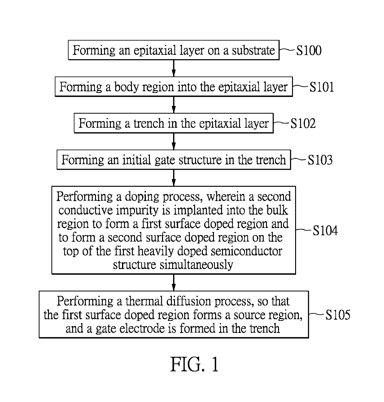
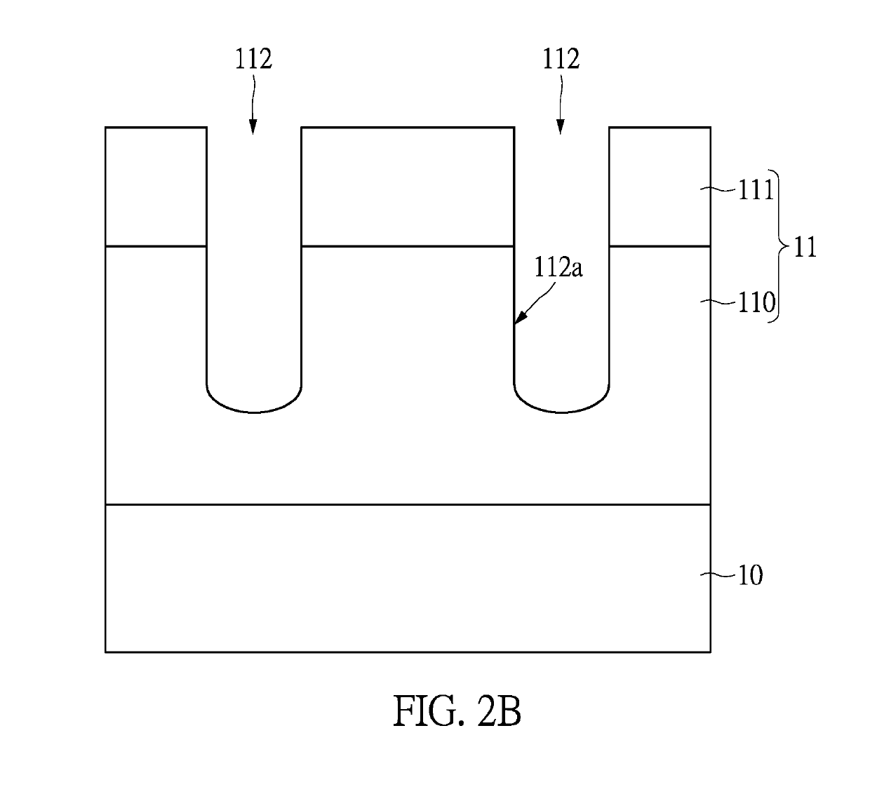
[0013]FIG. 1 shows a flow diagram of a manufacturing method of a trench power semiconductor device according to an exemplary embodiment of the present disclosure. Referring to FIGS. 2A-2J, which individually show local sectional views of a trench power semiconductor device in each step of the manufacturing method according to an exemplary embodiment of the present disclosure.

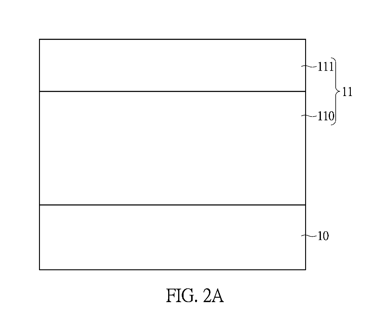
[0014]In step S100, an epitaxial layer 11 is formed on a substrate 10, as shown in FIG. 2A. FIG. 2A illustrates the substrate 10, and the epitaxial layer 11 is formed on the substrate 10. The substrate 10 may exemplarily be a silicon substrate having a first heavily doped region with high doping concentration as a drain of the t...


PUM


Abstract

A trench power semiconductor device and a manufacturing method thereof are provided. The trench power semiconductor device includes a substrate, an epitaxial layer disposed on the substrate, and a gate structure. The epitaxial layer has at least one trench formed therein, and the gate structure is disposed in the trench. A gate structure includes a lower doped region and an upper doped region disposed above the lower doped region to form a PN junction. The concentration of the impurity decreases along a direction from a peripheral portion of the upper doped region toward a central portion of the upper doped region.

Description

BACKGROUND1. Technical Field[0001]The present disclosure is related to a power semiconductor and a manufacturing method thereof, and in particular, to a trench power transistor and a manufacturing method thereof.2. Description of Related Art[0002]Current power metal-oxide-semiconductor field-effect transistors (power MOSFET) are designed to have a vertical structure to improve the packing density. The working loss of power MOSFFT is categorized into switching loss and conducting loss. In addition, the intrinsic gate-to-drain capacitance (Cgd) is one of the important parameters affecting switching loss. When the intrinsic gate-to-drain capacitance is too high, the switching loss increases, which may limit the switching speed of the power trench MOSFET and may lead to the trench power MOSFET being unfavorable to be implemented in high frequency circuits.SUMMARY[0003]The object of the present disclosure is to provide a trench power semiconductor device and a manufacturing method thereo...

Claims


Application Information

Patent Timeline
Patent Type & Authority Patents(United States)
IPC IPC(8): H01L29/49H01L29/78H01L21/28H01L29/06H01L29/10H01L29/423H01L29/51
CPCH01L21/28114H01L29/7813H01L29/66734H01L29/42368H01L29/42376H01L29/4925H01L29/513H01L29/518H01L21/28035H01L21/28158H01L29/0646H01L29/1095H01L29/512
Inventor HSU, HSIU-WEN
Owner SUPER GROUP SEMICON
Why Eureka
Try Eureka