Trench power MOSFET and manufacturing method thereof

a technology of power mosfet and manufacturing method, which is applied in the direction of transistors, electrical devices, semiconductor devices, etc., can solve the problems of limiting switching speed, high packing density, and lower on-state resistance, and achieve the effect of reducing the effective capacitan

Active Publication Date: 2017-01-03
SUPER GROUP SEMICON
View PDF5 Cites 0 Cited by
  • Summary
  • Abstract
  • Description
  • Claims
  • Application Information

AI Technical Summary

Benefits of technology

[0006]The object of the present invention is to provide a trench power MOSFET and a manufacturing method thereof, which can decrease the effective capacitance between the gate and the drain by using a gate having a PIN, P+ / N−, or N+ / P− junction formed therein.
[0009]To sum up, the trench power MOSFET and the manufacturing method thereof in accordance with the present invention make the formation of a PIN, P+ / N− or N+ / P− junction in the gate. Since a junction capacitance (Cj) of the PIN, P+ / N− or N+ / P− junction is generated under reverse bias, and the junction of capacitance is in series with the parasitic capacitance (Cp), the effective capacitance between the gate and the drain can be reduced.

Problems solved by technology

The power MOSFET having trench gate structure not only results in higher packing density, but also has lower on-state resistance.
When the intrinsic gate-to-drain capacitance is too high, the switching loss increases, which may limit the switching speed of the power trench MOSFET and may lead to the trench power MOSFET being unfavorable to be implemented in high frequency circuits.

Method used


Image

  • Trench power MOSFET and manufacturing method thereof
  • Trench power MOSFET and manufacturing method thereof
  • Trench power MOSFET and manufacturing method thereof

Examples


Embodiment Construction

[0018]The aforementioned illustrations and following detailed descriptions are exemplary for the purpose of further explaining the scope of the present invention. Other objectives and advantages related to the present invention will be illustrated in the subsequent descriptions and appended drawings. In reference to the disclosure herein, for purposes of convenience and clarity only, directional terms, such as, top, bottom, left, right, up, down, over, above, below, beneath, rear, front, distal, and proximal are used with respect to the accompanying drawings. Such directional terms should not be construed to limit the scope of the invention in any manner. In addition, the same reference numerals are given to the same or similar components.

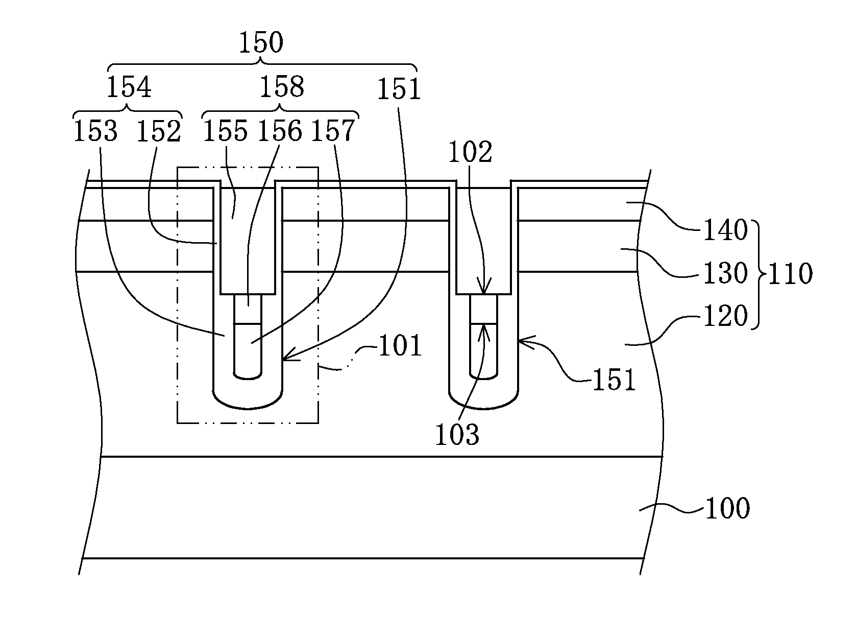
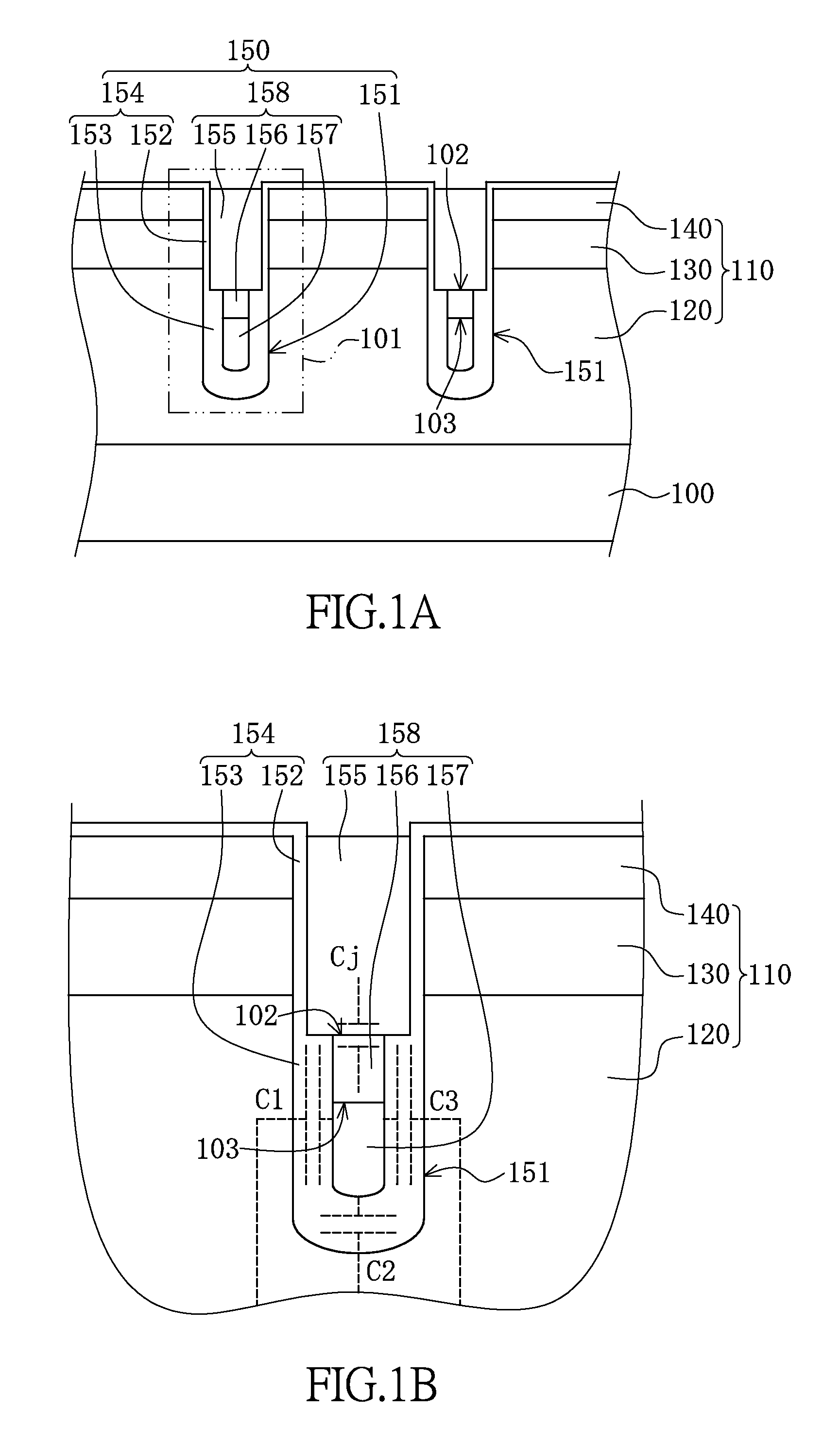
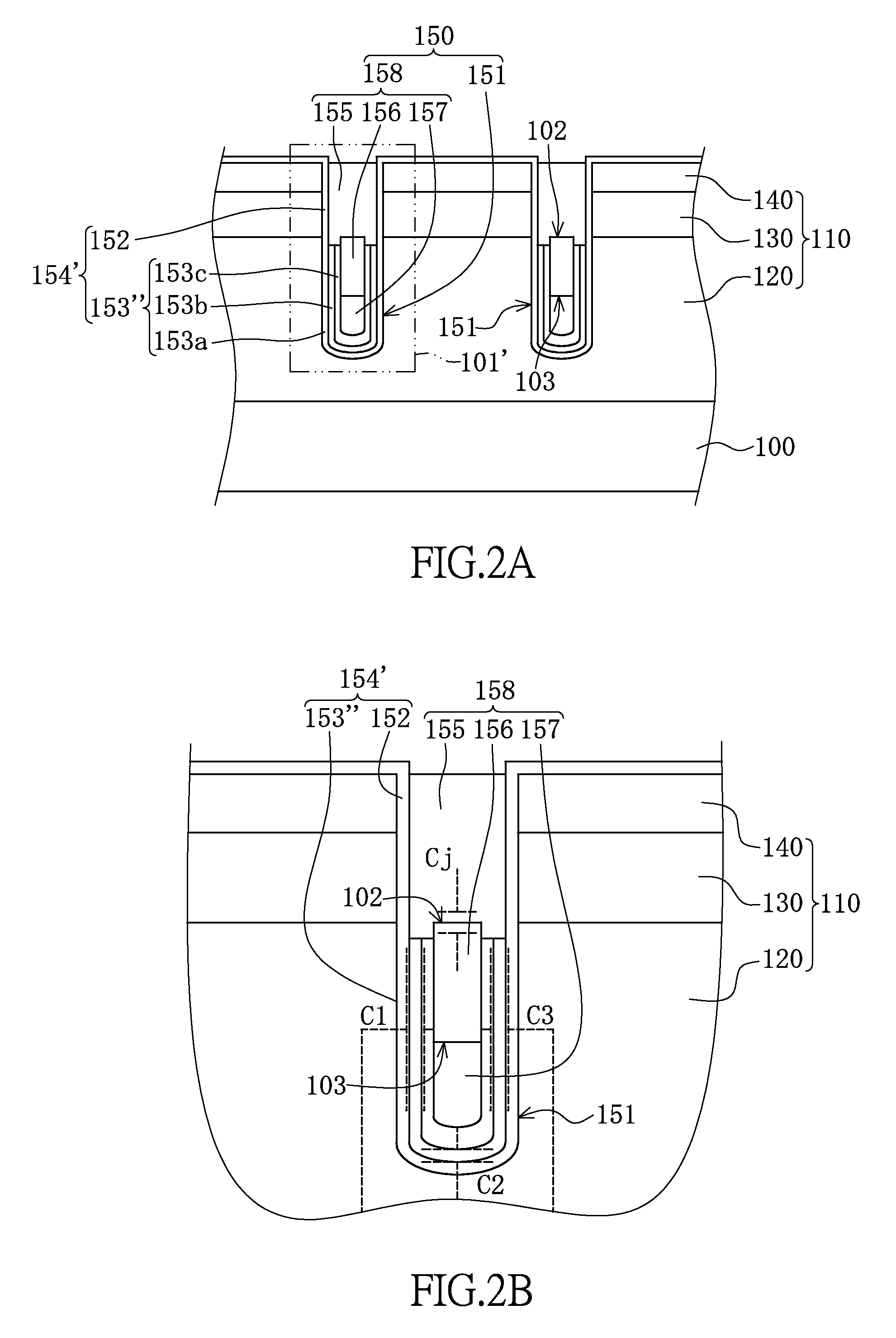
[0019]FIG. 1A shows a local sectional view of a trench power MOSFET provided in accordance with an embodiment of the present invention. The trench power MOSFET includes a substrate 100, an epitaxial layer 110 and a plurality of trench transistor un...


PUM


Abstract

A trench power MOSFET and a manufacturing method thereof are provided. The gate of the trench power MOSFET includes an upper doped region, a lower doped region and a middle region interposed therebetween. The upper has a conductive type reverse to that of the lower doped region, and the middle region is an intrinsic or lightly-doped region to form a PIN, P+ / N− or N+ / P− junction. As such, when the trench power MOSFET is in operation, a junction capacitance formed at the PIN, P+ / N− or N+ / P− junction is in series with the parasitic capacitance. Accordingly, the gate-to-drain effective capacitance may be reduced.

Description

BACKGROUND OF THE INVENTION[0001]1. Field of the Invention[0002]The present invention relates to a power metal-oxide-semiconductor field-effect transistor (MOSFET) and manufacturing method thereof; in particular, to a trench power MOSFET and manufacturing method thereof.[0003]2. Description of Related Art[0004]Power metal-oxide-semiconductor field-effect transistors (Power MOSFET) are widely implemented in the switching devices of electric devices, such as power supply, rectifier or low voltage motor controllers and the like. The current power MOSFET is designed to have a vertical structure to improve the packing density. The power MOSFET having trench gate structure not only results in higher packing density, but also has lower on-state resistance. One of the advantages of the trench power MOSFET is that it is capable of controlling the operation of devices with low-power consumption.[0005]The working loss of power MOSFET is categorized into a switching loss and a conducting loss. ...

Claims


Application Information

Patent Timeline
Patent Type & Authority Patents(United States)
IPC IPC(8): H01L29/78H01L29/66H01L29/423H01L27/088H01L21/8234H01L29/10H01L29/51H01L29/08
CPCH01L29/4236H01L21/823437H01L21/823462H01L27/088H01L29/086H01L29/1095H01L29/42368H01L29/511H01L29/66734H01L29/7813H01L29/4916
Inventor HSU, HSIU-WEN
Owner SUPER GROUP SEMICON
Why Eureka
Try Eureka