Chip type high polymer electrostatic discharge protecting element and manufacturing method thereof

A technology for electrostatic discharge protection and component manufacturing, which is applied in the field of patch-type polymer ESD protection components and its manufacturing, can solve the problems of complex lead-out methods for connecting internal and external electrodes, signal attenuation and distortion, and small effective capacitance, etc., to achieve Meets ESD protection requirements, facilitates electrode graphic design, and has good connection effects

Active Publication Date: 2012-12-26
SHENZHEN SUNLORD ELECTRONICS
View PDF0 Cites 0 Cited by
  • Summary
  • Abstract
  • Description
  • Claims
  • Application Information

AI Technical Summary

Problems solved by technology

[0002] In the signal transmission port HDMI, HDMI1.3, USB3.0, IEEE1394B, low-voltage differential signaling (Low-voltage differential signaling, the abbreviation is LVDS), the ESD protection element itself has a certain capacitance, among which the varistor, transient The capacitance of the diode (Transient Voltage Suppressor, abbreviated as TVS) cannot be reduced enough to cause signal attenuation and distortion in the high-speed signal transmission line
The effective capacitance of the existing ESD protection components made of polymer pressure-sensitive materials is very small, and they all use inorganic ceramics or copper-clad laminates as the upper and lower substrates, which require high-end cutting equipment and high cost. The lead-out method is more complicated and difficult to manufacture

Method used


Image

  • Chip type high polymer electrostatic discharge protecting element and manufacturing method thereof
  • Chip type high polymer electrostatic discharge protecting element and manufacturing method thereof
  • Chip type high polymer electrostatic discharge protecting element and manufacturing method thereof

Examples


specific Embodiment approach 1

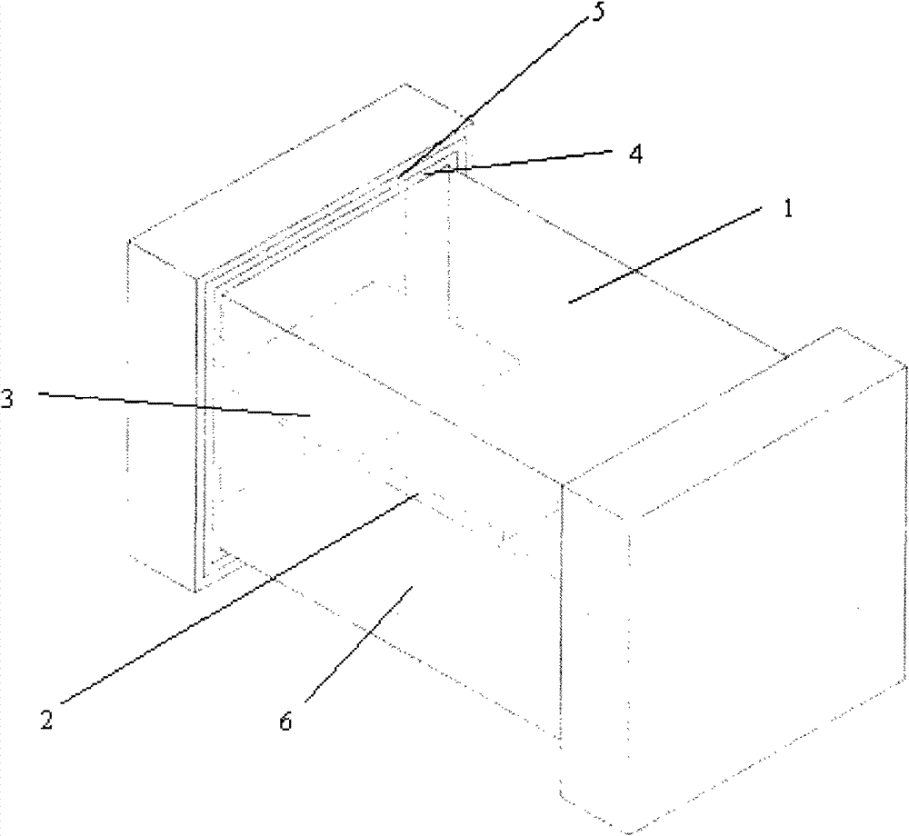
[0056] a kind of like Figure 1~3 The chip-type polymer electrostatic discharge protection component shown includes an upper substrate 1 , a lower substrate 6 , a core material 2 , two inner electrodes 3 , two terminal electrodes 4 and two electroplating layers 5 . The upper substrate 1, the lower substrate 6, and the core material 2 all belong to high molecular polymers, and all include a curing agent.

[0057] The two internal electrodes 3 are two internal electrodes opposing in the longitudinal direction, and the core material 2 is a core material filling a gap between the two internal electrodes 3 opposing in the longitudinal direction. The upper substrate 1 is an epoxy resin board, and the lower substrate 6 is an alumina ceramic board.

[0058] The core material 2 is a composite material, and the components and mass percentages of the core material slurry are as follows:

[0059] Epoxy resin 35.0%;

[0060] Silver powder 25.0%;

[0061] Silicon carbide 35.0%;

[0062] ...

specific Embodiment approach 2

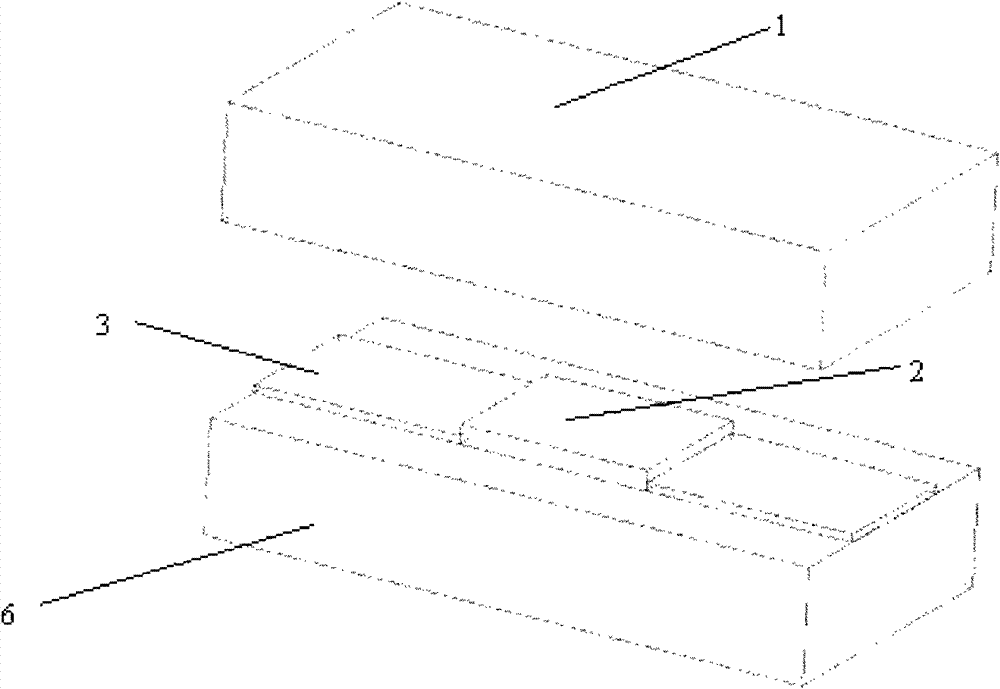
[0084] a kind of like Figure 4 The chip-type polymer electrostatic discharge protection component shown includes an upper substrate 1 , a lower substrate 6 , a core material 2 , two inner electrodes 3 , two terminal electrodes 4 and two plating layers 5 .

[0085] The composition and structure of the device is basically the same as that of Embodiment 1, the difference is:

[0086] The two internal electrodes 3 are two internal electrodes that intersect each other in the longitudinal direction, and the core material 2 is a core material that fills the gap between the two intersecting internal electrodes in the longitudinal direction. The lower substrate 1 and the lower substrate 6 are silicone resin plates.

[0087] Its manufacturing method is basically the same as specific embodiment one, and its difference is:

[0088] First prepare an internal electrode 3 , then prepare the core material 2 , and then prepare another internal electrode 3 .

[0089] The core material 2 is ...

specific Embodiment approach 3

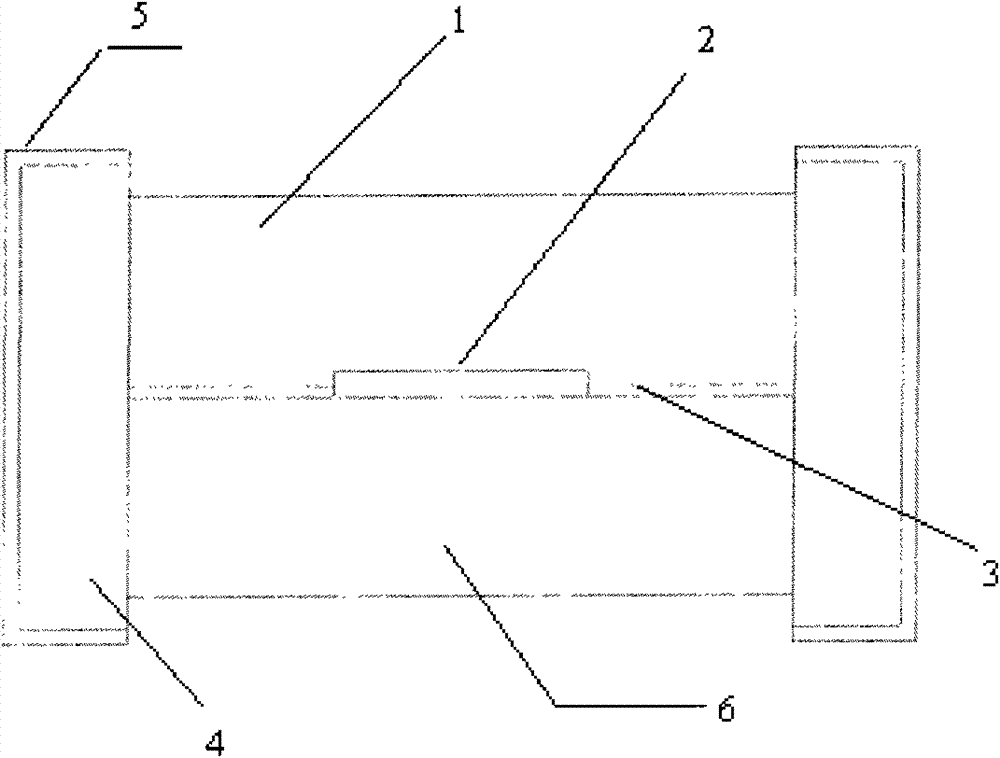
[0096] a kind of like Figure 5 , 6 The chip-type polymer electrostatic discharge protection component shown includes an upper substrate 1 , a lower substrate 6 , a core material 2 , two inner electrodes 3 , two terminal electrodes 4 and two plating layers 5 .

[0097] The composition and structure of the device is basically the same as that of Embodiment 1, the difference is:

[0098] The core material 2 is a core material that fills a through hole in the gap between two inner electrodes opposite in the length direction. The upper substrate 1 is an epoxy resin plate, and the lower substrate 6 is a glass-ceramic plate.

[0099] Its manufacturing method is basically the same as specific embodiment one, and its difference is:

[0100] Using a dicing and cutting machine, the glass-ceramic plate is cut into the lower substrate 6 according to the designed shape and size, and holes are opened on the lower substrate 6, and then the inner electrode 3 is prepared. When the core mate...


PUM

PropertyMeasurementUnit
widthaaaaaaaaaa

Abstract

The invention provides a chip type high polymer electrostatic discharge protecting element. Inner electrodes are one of two inner electrodes opposite to each other in a length direction and two inner electrodes staggered with each other in the length direction; and a core material is one of a core material filled in a gap between the two inner electrodes opposite to each other in the length direction, a core material filled in a gap between the two inner electrodes staggered with each other in the length direction, and a core material filled in a through hole in the gap between the two inner electrodes opposite to each other in the length direction. The manufacturing method sequentially comprises the following steps: (1) the preparation of slurry of the core material; (2) the preparation of a lower substrate; (3) the preparation of the inner electrodes; (4) the preparation of the core material; (5) the preparation of an upper substrate; (6) cutting of a chip; (7) the preparation of terminal electrodes; and (8) electroplating. A chip type ESD (Electrostatic Discharge) protecting device which has small size and very small effective capacitance can be manufactured; the requirements of high-speed signal transmission equipment on the ESD protection can be sufficiently met; the inner electrodes and the terminal electrodes are easier to connect, and the terminal electrodes are easier to lead out, therefore, the chip type high polymer electrostatic discharge protecting element is easy to manufacture; moreover; and the gap between the inner electrodes can be correspondingly adjusted according to the value of a trigger voltage in the design.

Description

technical field [0001] The present invention relates to electrostatic discharge (Electrostatic Discharge, abbreviated as ESD) protection, in particular to a patch type polymer ESD protection element and a manufacturing method thereof. Background technique [0002] In the signal transmission port HDMI, HDMI1.3, USB3.0, IEEE1394B, low-voltage differential signaling (Low-voltage differential signaling, the abbreviation is LVDS), the ESD protection element itself has a certain capacitance, among which the varistor, transient The capacitance of the diode (Transient Voltage Suppressor, abbreviated as TVS) cannot be reduced to a small enough value, resulting in attenuation and distortion of the signal in the high-speed signal transmission line. The effective capacitance of the existing ESD protection components made of polymer pressure-sensitive materials They are very small, and they use inorganic ceramics or copper-clad laminates as the upper and lower substrates, which require h...

Claims


Application Information

Patent Timeline
Patent Type & Authority Patents(China)
IPC IPC(8): H01L23/60H01L23/00H01L21/00C08L63/00C08L83/00
Inventor 冯志刚毛海波贾广平王小波师习恩成学军姚斌
Owner SHENZHEN SUNLORD ELECTRONICS
Why Eureka
Try Eureka