Semiconductor device

a technology of semiconductor devices and heat dissipation plates, which is applied in the direction of semiconductor devices, semiconductor/solid-state device details, electrical equipment, etc., can solve the problems of deterioration of heat dissipation plates and products, and achieve the effect of improving product attachmen

Active Publication Date: 2019-12-10
MITSUBISHI ELECTRIC CORP
View PDF7 Cites 0 Cited by
  • Summary
  • Abstract
  • Description
  • Claims
  • Application Information

AI Technical Summary

Benefits of technology

[0006]It is an object of the present invention to provide a technique for improving product attachment.
[0008]The angle A is reduced. This prevents a location in which the other attachment hole in the attachment portion of the case is disposed from detaching upward from a surface of the heat sink. Consequently, the product attachment is improved.

Problems solved by technology

The flexible heat dissipation plate unfortunately deteriorates a product with time.
However, the technique in Japanese Utility Model Application Laid-Open No. 4-46552 involves unfavorable product attachment because the technique fails to reflect the warpage of the heat dissipation plate.

Method used


Image

  • Semiconductor device
  • Semiconductor device
  • Semiconductor device

Examples


first preferred embodiment

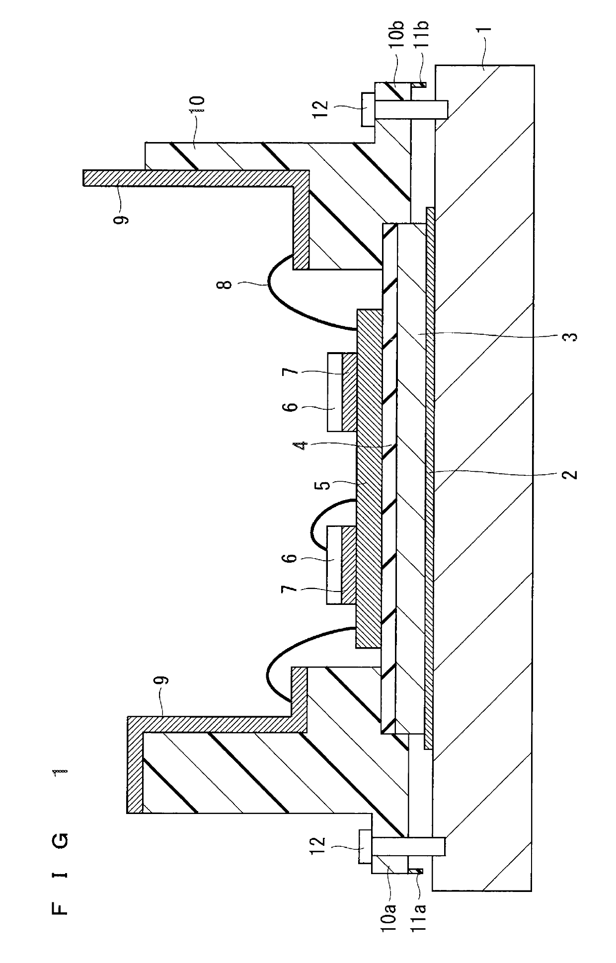
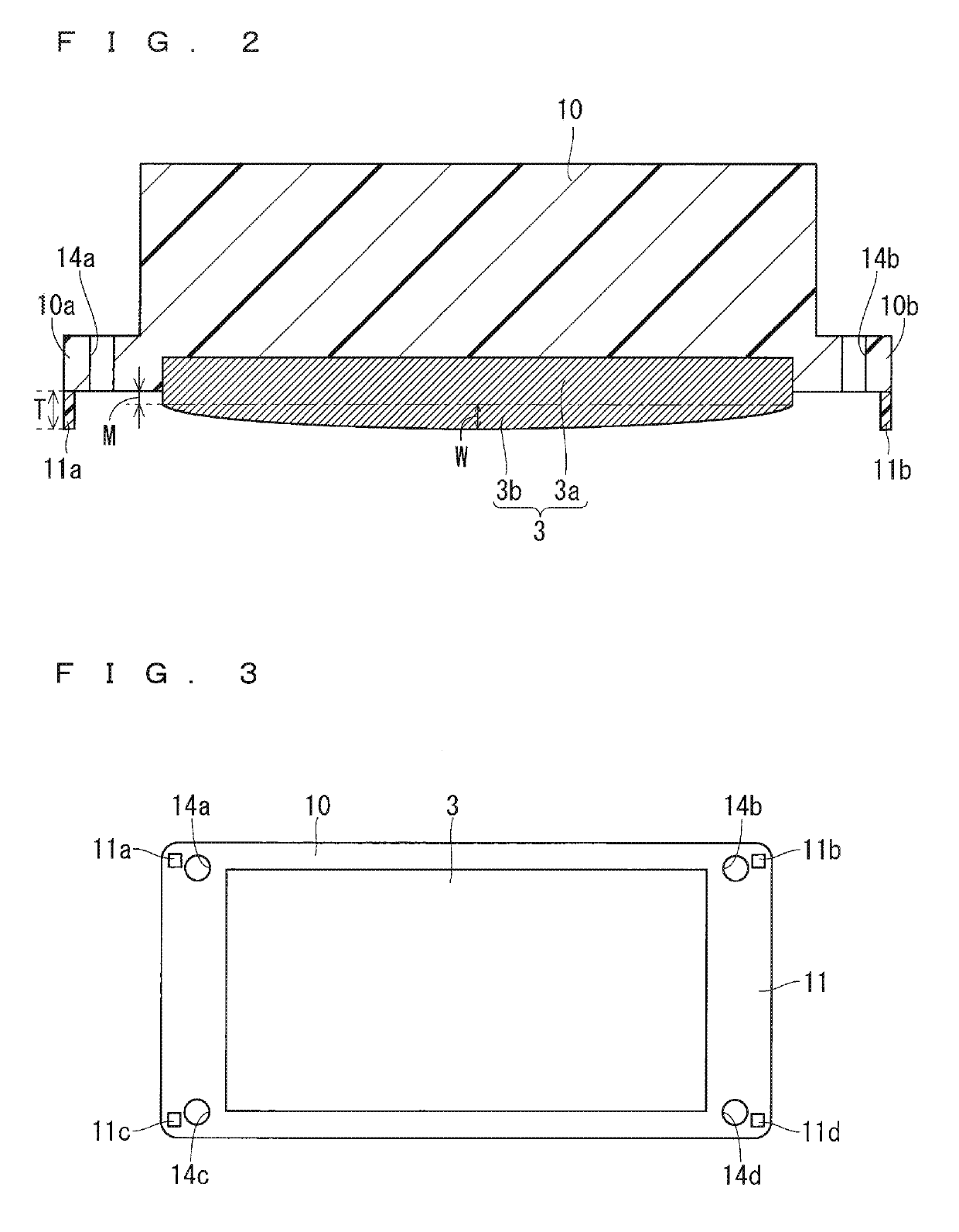
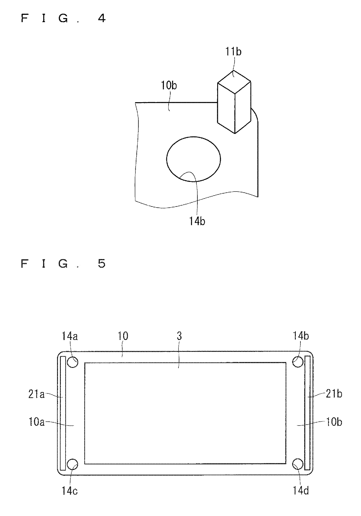
[0031]The following describes a first preferred embodiment of the present invention with reference to the drawings. FIG. 1 is a cross-sectional view of a semiconductor device according to the first preferred embodiment. FIG. 2 is a cross-sectional view of the semiconductor device with a heat sink 1 removed therefrom. FIG. 3 is a bottom view of the semiconductor device with the heat sink 1 removed therefrom. FIG. 4 is a perspective bottom view of a projection 11b and its surrounding portion.

[0032]As illustrated in FIG. 1, the semiconductor device is a power semiconductor device, and includes the heat sink 1, a heat dissipation plate 3, a plurality of semiconductor elements 6, a plurality of metal terminals 9, a case 10, and screws 12.

[0033]The heat dissipation plate 3 is disposed above the heat sink 1. More specifically, the heat dissipation plate 3 has a lower surface provided with a thermally conductive material 2, and is disposed on the upper surface of the heat sink 1 with the th...

second preferred embodiment

[0051]The following describes a semiconductor device according to a second preferred embodiment. FIG. 9 is a simple cross-sectional view of the semiconductor device as screwed according to the second preferred embodiment. FIG. 10 is a perspective bottom view of a projection 31 and its surrounding portion. It is noted that the same components between the first preferred embodiment and the second preferred embodiment are denoted by the same symbols, and will not be elaborated upon here.

[0052]In the second preferred embodiment, four projections 31 are bent outward by stress in the fastening of the screws 12, as illustrated in FIGS. 9 and 10.

[0053]The projections 31 are each made of a resin, such as a PPS. The projection 31 is provided with a horizontally extending cutout 31a in a position adjacent to the attachment hole 14b positioned in the surrounding portion of the projection 31. The cutout 31a facilitates the bending of the projection 31. The easy bending of the projection 31 thank...

third preferred embodiment

[0057]The following describes a semiconductor device according to a third preferred embodiment. FIG. 11 is a perspective bottom view of a projection 41 and its surrounding portion of the semiconductor device according to the third preferred embodiment. FIG. 12 is a cross-sectional view of the projection 41 and its surrounding portion. It is noted that the same components between the first and second preferred embodiments, and the third preferred embodiment are denoted by the same symbols, and will not be elaborated upon here.

[0058]In the third preferred embodiment, four projections 41 are bent outward by stress in the fastening of the screws 12, as illustrated in FIGS. 11 and 12.

[0059]The projections 41 are each made of a resin, such as a PPS. The projection 41 is provided with an inclined portion 41a inclined toward an attachment-hole-14b side with respect to the lower surface of the attachment portion 10b so as to have a smaller width in the distal end portion of the projection 41...


PUM


Abstract

Provided is a technique for improving product attachment. In a semiconductor device, the following expression is satisfied by an angle A formed by an imaginary line connecting two attachment holes together and an imaginary line connecting together a lowest point of one of two projections positioned in a surrounding portion of one of the two attachment holes and a contact point between a bulge and a heat sink, with a screw fastened to the heat sink through the one attachment hole, where M represents a vertical direction between the lower end of a body and the lower end of a case, where W represents a bulge amount of the bulge, where T represents a height of the projection, where L represents a horizontal distance from the outer peripheral end of the case to the outer peripheral end of the heat dissipation plate: 0<A<arctan((M+W−T) / L).

Description

BACKGROUND OF THE INVENTIONField of the Invention[0001]The present invention relates to semiconductor devices, and more particularly, to a power semiconductor device including a power chip.Description of the Background Art[0002]In a power semiconductor device including a power chip, efficiently dissipating heat generated in the power chip to an external structure, such as a heat sink is highly important. The use of a thermally conductive material enables efficient heat dissipation when the body of the semiconductor device is attached to the heat sink.[0003]Provided is a structure in which the center portion of a heat dissipation plate provided with the power chip is brought into contact with the heat sink through screwing in order to accelerate heat dissipation from the thermally conductive material to the heat sink (e.g., Japanese Patent Application Laid-Open No. 4-233752 and Japanese Utility Model Application Laid-Open No. 4-46552).[0004]The technique in Japanese Patent Applicatio...

Claims


Application Information

Patent Timeline
Patent Type & Authority Patents(United States)
IPC IPC(8): H01L23/40H01L23/04H01L23/433H01L23/373
CPCH01L23/433H01L23/04H01L23/4006H01L23/3735H01L2924/19107H01L2023/4025H01L2023/4068H01L2023/4087H01L2023/4043H01L2224/48091H01L2924/00014H01L2224/73265H01L23/40H01L23/041
Inventor OKADA, KAZUYAMURAOKA, HIROKIMASUDA, KOICHISHIMIZU, YASUTAKAIZUMI, SHOJI
Owner MITSUBISHI ELECTRIC CORP
Why Eureka
Try Eureka