Method for rewriting data in nonvolatile memory and semiconductor device

a nonvolatile memory and data rewriting technology, applied in the direction of memory adressing/allocation/relocation, instruments, digital storage, etc., can solve the problem of long time-consuming data rewriting process

Active Publication Date: 2020-02-11
LAPIS SEMICON CO LTD
View PDF28 Cites 0 Cited by
  • Summary
  • Abstract
  • Description
  • Claims
  • Application Information

AI Technical Summary

Benefits of technology

[0007]It is therefore an object of the present invention is to provide a method for rewriting data in nonvolatile memory and semiconductor device which are capable of realizing data rewriting within shorter time.
[0012]In conventional method for rewriting data, a set of process is needed to be performed for rewriting a part of data pieces in a block. The set of process is composed of copying data except for the above data piece which is written in the writing destination block to the temporary storage block, and setting the temporary storage block to be in an externally accessible state. In the present invention, data can be rewritten within shorter time than in the conventional method.
[0014]It is therefore, the physical address indicating the temporary storage block which is a target of an accessing can be obtained more rapidly than in the conventional method. In the conventional method, the temporary storage block corresponding to the target of an accessing is searched by determining whether it is an object of accessing or not with respect to each of the plurality of temporary storage blocks.

Problems solved by technology

The data rewriting process takes long time.

Method used


Image

  • Method for rewriting data in nonvolatile memory and semiconductor device
  • Method for rewriting data in nonvolatile memory and semiconductor device
  • Method for rewriting data in nonvolatile memory and semiconductor device

Examples


Embodiment Construction

[0030]An embodiment of the present invention will now be described below in detail with reference to the drawings.

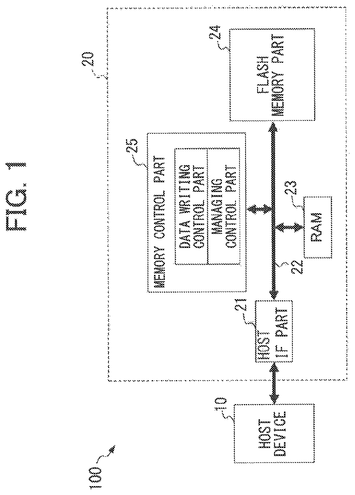
[0031]FIG. 1 is a block diagram showing a configuration of information processing system 100 having a host device 10 and a nonvolatile memory 20 as a semiconductor device according to the present invention.

[0032]The host device 10 performs information processing on the basis of data stored in the nonvolatile memory 20. The host device 10 supplies the nonvolatile memory 20 with a writing command, an address indicating writing destination, an incoming data to be written, a read out command, and an address for reading out.

[0033]The nonvolatile memory 20 has a host interface part 21 (hereinafter referred to as a host IF part 21), an internal bus 22, a RAM (Random Access Memory) 23, a flash memory part 24, and a memory control part 25.

[0034]The host IF part 21 supplies the internal bus 22 with the writing command, the address indicating writing destination and the incoming da...


PUM


Abstract

In the present invention, a vacant block which is unwritten is identified as a temporary storage block when a writing destination block has already data written. Then, data writing step writing an incoming data to be written into the temporarily storage block, managing step including assigning a pair of the writing destination block and the temporarily storage block an index number which corresponds to the pair, and generating a management table which indicates the index number associating with a physical address indicating a physical position of the temporarily storage block in the nonvolatile memory are performed. In the data writing step, the physical address which corresponds to the index number assigned to the writing destination block is obtained from the management table. The incoming data to be written is written into the temporary storage block indicated by the physical address.

Description

BACKGROUND1. Field[0001]The present invention relates to a method for rewriting data which is written in a memory, particularly in a nonvolatile memory, and to a semiconductor device which includes a nonvolatile memory.2. Description of the Related Art[0002]A NAND type flash memory (hereinafter referred to as NAND memory) as a nonvolatile semiconductor memory writes and reads data in increments of a page. The NAND memory erases data in increments of a block constituted by a plurality of pages.[0003]In the NAND memory, data cannot be overwritten on a page with data written thereon. For example, rewriting of data is performed in a manner as follows (for example, Japanese Patent Application Laid-Open No. 2009-134682).[0004]At first, incoming data to be written is written in a vacant block which is not written with data. Then, all data which is not to be rewritten is read out from a writing destination block which is specified by an address. The data which is read out is written in the ...

Claims


Application Information

Patent Timeline
Patent Type & Authority Patents(United States)
IPC IPC(8): G11C16/10G06F12/02G11C16/04G11C11/56
CPCG11C16/10G06F12/0246G11C11/5628G06F2212/7201G11C16/0483G06F2212/7203
Inventor WATANABE, TOMOMI
Owner LAPIS SEMICON CO LTD
Why Eureka
Try Eureka