Supercharge Your Innovation With Domain-Expert AI Agents!

Static random access memory structure

a random access and memory technology, applied in the field of static random access memory (sram) structure, can solve the problems of difficult for the current sram architecture to produce desirable patterns, and achieve the effect of reducing errors caused by the difference of signal path length, high symmetry arrangement, and reducing the number of errors

Active Publication Date: 2020-02-11
UNITED MICROELECTRONICS CORP
View PDF10 Cites 0 Cited by
  • Summary
  • Abstract
  • Description
  • Claims
  • Application Information

AI Technical Summary

Benefits of technology

[0007]One feature of the present invention is that the first pass gate transistor and the second pass gate transistor share the same fin structure. Likewise, the third pass gate transistor and the fourth pass gate transistor share the same fin structure. Applicants have found that by the above configuration, the elements have high symmetry arrangement, and when the signal is generated, the signal path length of each pass gate transistor is substantially equal. Therefore, in the operation of static random access memory, the errors caused by the difference of the signal path length can be reduced, thereby improving the performance of the static random access memory.

Problems solved by technology

However, as gap of the exposure process decreases, it has been difficult for the current SRAM architecture to produce desirable patterns.

Method used


Image

  • Static random access memory structure
  • Static random access memory structure
  • Static random access memory structure

Examples


Embodiment Construction

[0016]To provide a better understanding of the present invention to users skilled in the technology of the present invention, preferred embodiments are detailed as follows. The preferred embodiments of the present invention are illustrated in the accompanying drawings with numbered elements to clarify the contents and the effects to be achieved.

[0017]Please note that the figures are only for illustration and the figures may not be to scale. The scale may be further modified according to different design considerations. When referring to the words “up” or “down” that describe the relationship between components in the text, it is well known in the art and should be clearly understood that these words refer to relative positions that can be inverted to obtain a similar structure, and these structures should therefore not be precluded from the scope of the claims in the present invention.

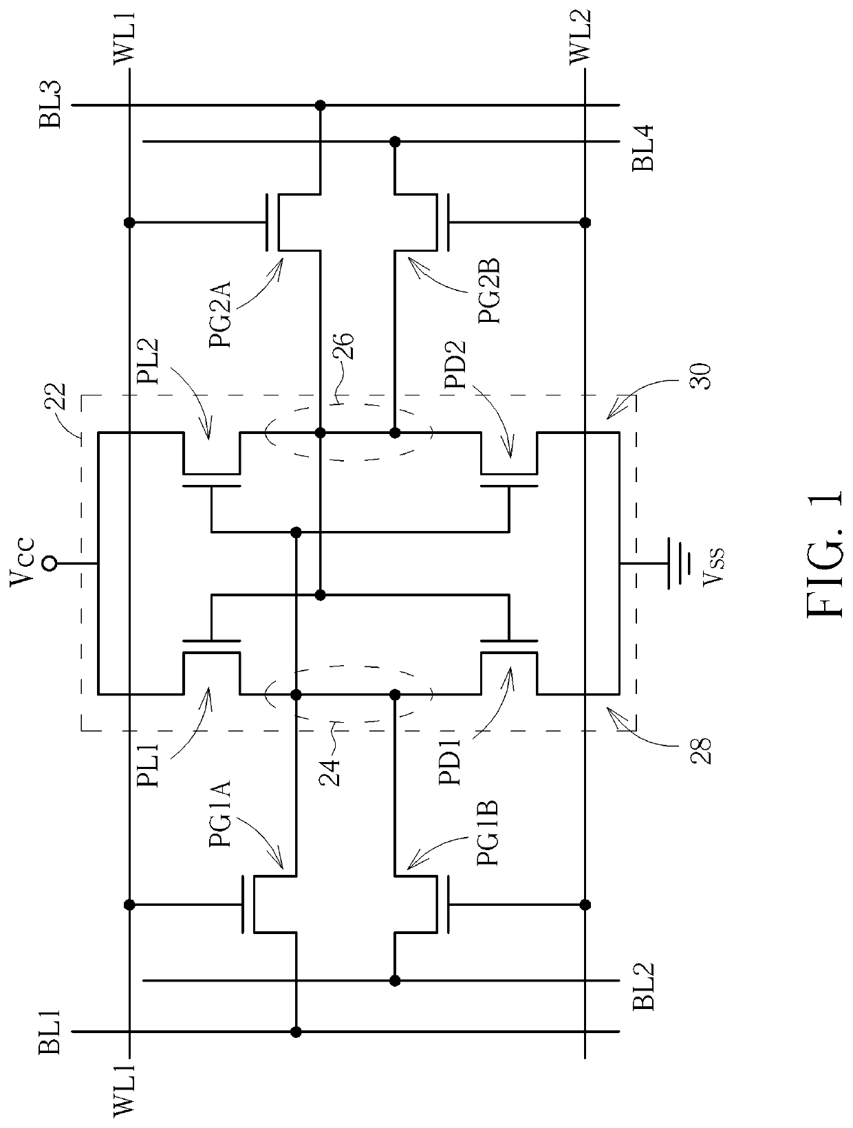
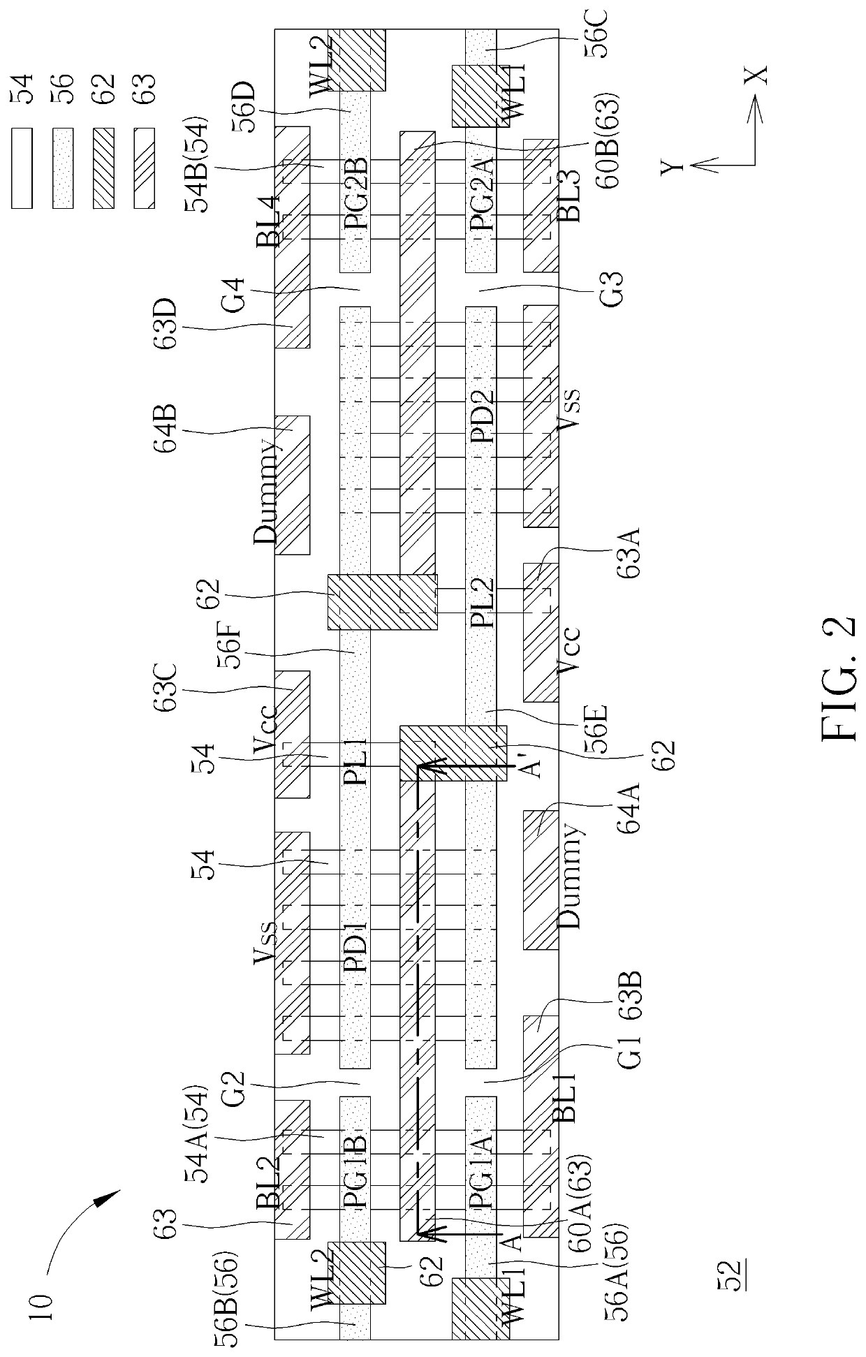
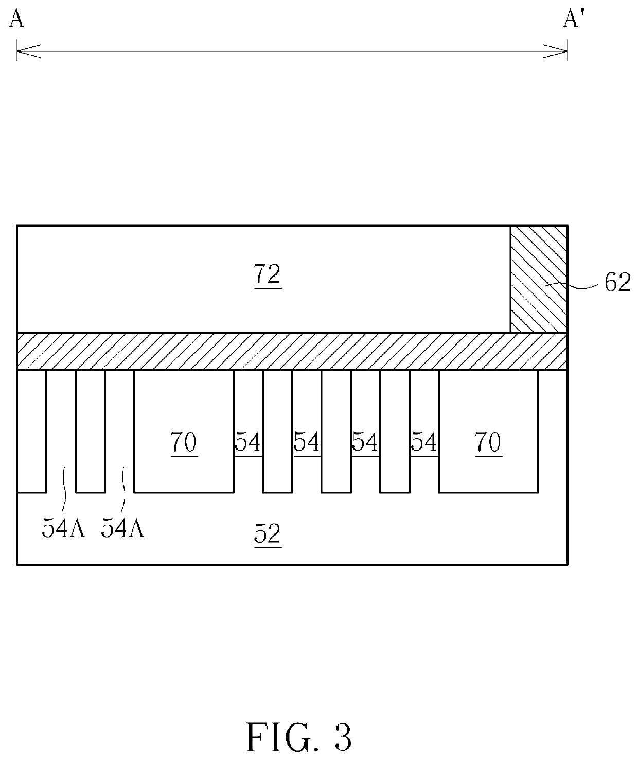
[0018]Referring to FIGS. 1-2, FIG. 1 illustrates a circuit diagram of an eight-transistor SRAM (8T-...


PUM


Abstract

A layout pattern of a static random access memory (SRAM) includes a substrate, a first pull-up transistor (PL1), a first pull-down transistor (PD1), a second (PL2), and a second pull-down transistor (PD2) on the substrate, and a first pass gate transistor (PG1A), a second pass gate transistor (PG1B), a third pass gate transistor (PG2A) and a fourth pass gate transistor (PG2B), wherein the PG1A and the PG1B comprise a first fin structure, the PG2A and the PG2B comprise a second fin structure, a first local interconnection layer disposed between the PG1A and the PG1B and disposed on the fin structures of the PL1 and the PD1, a second local interconnection layer disposed between the PG2A and the PG2B and disposed between the fin structures of the PL2 and the PD2, the first local interconnection layer and the second local interconnection layer are monolithically formed structures respectively.

Description

CROSS REFERENCE TO RELATED APPLICATIONS[0001]This application is a continuation in part application of U.S. patent application Ser. No. 15 / 795,247 filed Oct. 26, 2017, which is herein incorporated by reference in its entirety.BACKGROUND OF THE INVENTION1. Field of the Invention[0002]The invention relates to a static random access memory (SRAM) structure, and more particularly, to a SRAM having the advantages of higher yield and faster read speed.2. Description of the Prior Art[0003]An embedded static random access memory (SRAM) comprises a logic circuit and a static random access memory connected to the logic circuit. SRAM is a kind of volatile memory cell, which means it preserves data only while power is continuously applied. SRAM is built of cross-coupled inverters that store data during the time that power remains applied, unlike dynamic random access memory (DRAM) that needs to be periodically refreshed. Because of its high access speed, SRAM is also used in computer systems as...

Claims


Application Information

Patent Timeline
Patent Type & Authority Patents(United States)
IPC IPC(8): H01L27/11G11C11/412H01L27/02G11C8/14G11C7/18G11C5/06H01L27/092H01L27/12
CPCG11C11/412H01L27/1104G11C8/14G11C7/18G11C5/06H01L27/0207H01L27/0924H01L27/1211H10B10/12
Inventor WANG, SHU-RULUNG, CHING-CHENGKUO, YU-TSECHEN, CHIEN-HUNGHUANG, CHUN-HSIENHUANG, LI-PINGTSENG, CHUN-YENCHUANG, MENG-PING
Owner UNITED MICROELECTRONICS CORP
Features
  • R&D
  • Intellectual Property
  • Life Sciences
  • Materials
  • Tech Scout
  • Unparalleled Data Quality
  • Higher Quality Content
  • 60% Fewer Hallucinations
Learn More