Method of forming memory capacitor

a memory capacitor and capacitor technology, applied in the direction of capacitors, semiconductor devices, electrical apparatus, etc., can solve the problems of low storage capacity, high refresh frequency, affecting the performance of dram devices, etc., and achieve the effect of improving accuracy and high reliability

Active Publication Date: 2020-02-11
UNITED MICROELECTRONICS CORP +1
View PDF30 Cites 0 Cited by
  • Summary
  • Abstract
  • Description
  • Claims
  • Application Information

AI Technical Summary

Benefits of technology

[0005]The present invention therefore provides a method of forming memory capacitor, which is able to increase the reliability of the crown-type electrode.
[0008]The method of forming a capacitor provided by the present invention uses a soft etching process to upgrade the accuracy when forming the bottom electrode layer. Accordingly, a capacitor structure of a memory device with higher reliability can therefore be obtained.

Problems solved by technology

However, the reduction of the area of each memory cell leads to lower storage capability of the memory cell, which causes high refresh frequency and therefore affects the performance of the DRAM device.
However, because of the complexity of the fabrication process of forming the capacitor, when using conventional photolithography to form said crown-type stacked capacitors, it is usually limited to obtain a sidewall structure with desired depth and configuration in the crown-type stacked capacitors.
The situation has limited the storage capacitances and the access speed in the memory device, becoming a problem that needs to be solved in current memory industry.

Method used


Image

  • Method of forming memory capacitor
  • Method of forming memory capacitor
  • Method of forming memory capacitor

Examples


Embodiment Construction

[0011]To provide a better understanding of the presented invention, preferred embodiments will be described in detail. The preferred embodiments of the present invention are illustrated in the accompanying drawings with numbered elements.

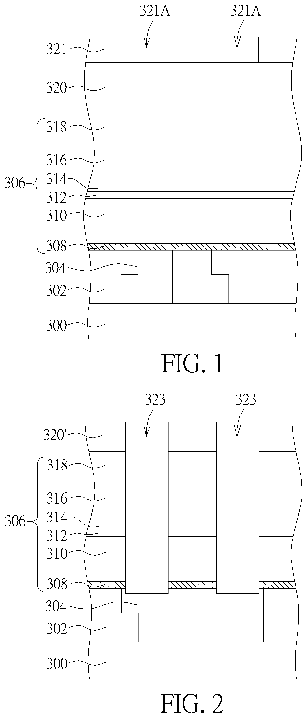
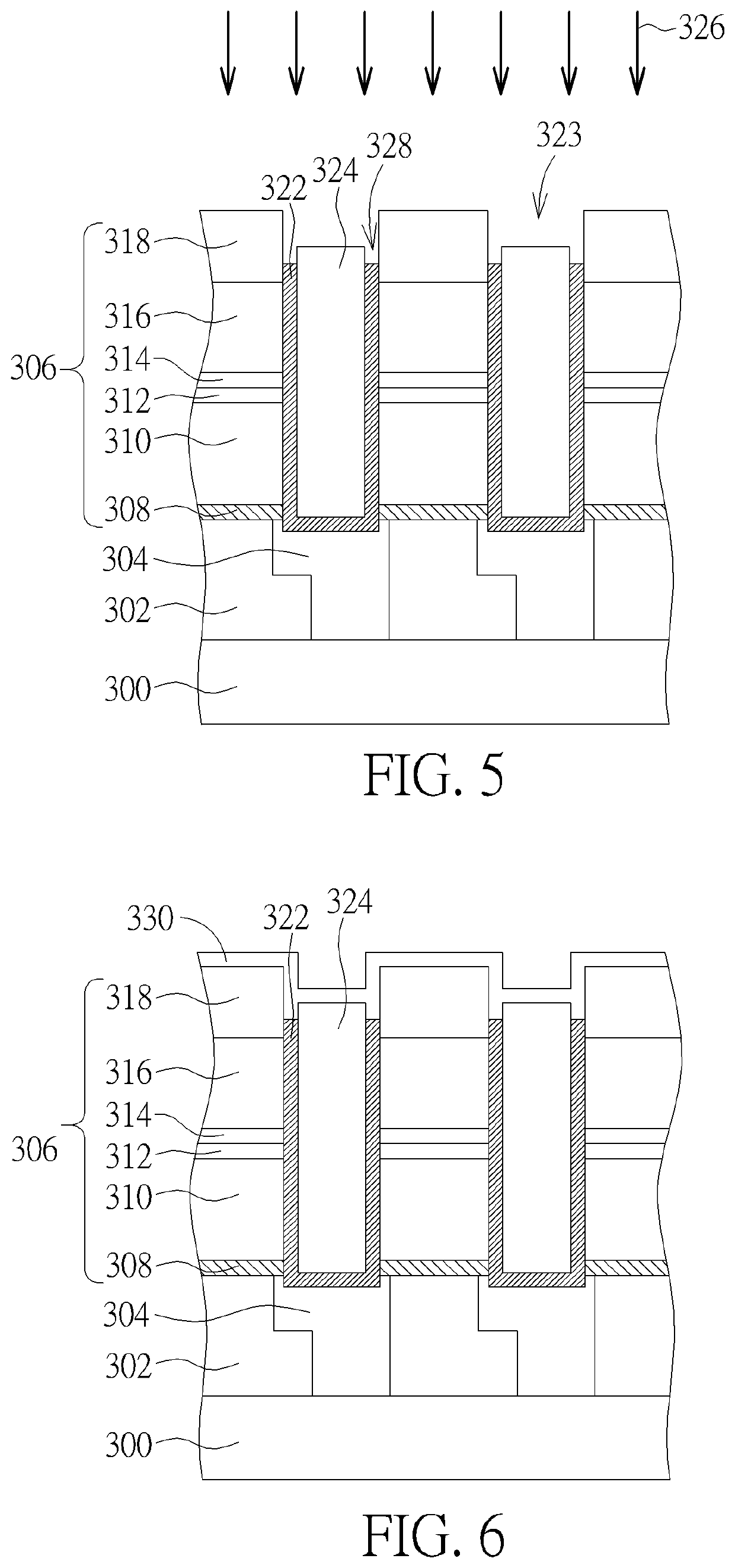
[0012]Please refer to FIG. 1 to FIG. 10, which are schematic diagrams showing the method of forming a memory capacitor according to one embodiment of the present invention. As shown in FIG. 1, a substrate 300 is provided. The substrate 300 may include a substrate having a semiconductor material, such as a silicon substrate, an epitaxial silicon substrate, a silicon germanium substrate, a silicon carbide substrate or a silicon-on-insulator (SOI) substrate. In one embodiment, the semiconductor substrate may have a plurality of electronic components such as access transistors (not shown) disposed thereon. In one embodiment, the access transistor can include a horizontal gate, a recess gate, or a vertical gate. Next, a dielectric layer 302 and a plurali...


PUM

PropertyMeasurementUnit
wavelengthaaaaaaaaaa
sizesaaaaaaaaaa
areaaaaaaaaaaa

Abstract

The present invention relates to a method of forming a memory capacitor. A substrate is provided with a plurality of storage node contacts. A patterned supporting structure is formed on the substrate, following by forming a bottom electrode conformally on surface of plural openings in the patterned supporting structure, thereby contacting the storage node contacts. A sacrificial layer is formed in the opening. A soft etching process is performed to remove the bottom electrode on top and partial sidewall of the patterned supporting structure, wherein the soft etching process includes using a fluoride containing compound, a nitrogen and hydrogen containing compound and an oxygen containing compound. The sacrificial layer is completely removed away. A capacitor dielectric layer and a top electrode are formed on the bottom electrode layer.

Description

BACKGROUND OF THE INVENTION1. Field of the Invention[0001]The present invention relates to a method of forming a memory capacitor, and more particularly, to a method of forming a memory capacitor containing a soft etching process.2. Description of the Prior Art[0002]A dynamic random access memory (DRAM) device is constituted by many memory cells. Generally, the memory cell is a semiconductor memory device with an access transistor and a storage capacitor. Each memory cell can store one bit data by storing electric charges in the storage capacitor.[0003]In general, the storage capacitor is constituted by an upper electrode, a dielectric layer, and a lower electrode. The storage capability of the storage capacitor is proportion to an overlapping area between the upper / lower electrodes and the dielectric layer. Since modern electrical products are developed with minimized sizes thereof, the area of each memory cell tends to be reduced, so that the DRAM device can be designed with high ...

Claims


Application Information

Patent Timeline
Patent Type & Authority Patents(United States)
IPC IPC(8): H01L21/3213H01L27/08H01L49/02H01L27/108
CPCH01L27/0805H01L28/92H01L21/32139H01L21/32133H01L27/10852H01L28/40H01L28/60H10B12/37H10B12/038H01L28/55H01L21/32135H01L21/32134H10B12/315H10B12/033
Inventor CHANG, FENG-YILEE, FU-CHECHEN, CHIEH-TE
Owner UNITED MICROELECTRONICS CORP
Why Eureka
Try Eureka