Supercharge Your Innovation With Domain-Expert AI Agents!

Active matrix substrate, display panel, and display device provided with same

a technology of active matrix substrate and display panel, which is applied in the direction of identification means, semiconductor devices, instruments, etc., can solve the problems of short circuits near the display panel and display defects

Active Publication Date: 2020-03-03
SHARP KK
View PDF7 Cites 0 Cited by
  • Summary
  • Abstract
  • Description
  • Claims
  • Application Information

AI Technical Summary

Benefits of technology

This configuration effectively isolates regions where short circuits may occur due to mechanical dividing, preventing display defects and allowing for reliable laser scanning to remove short circuits without impacting the display area.

Problems solved by technology

However, when a display panel provided with an active matrix substrate is mechanically divided in order to alter the size, a short circuit may occur near the dividing line.
This short circuit then causes a display defect in the display panel after the size alteration.

Method used


Image

  • Active matrix substrate, display panel, and display device provided with same
  • Active matrix substrate, display panel, and display device provided with same
  • Active matrix substrate, display panel, and display device provided with same

Examples


embodiment 1

[0026]Hereinafter, one embodiment of the present disclosure will be described in detail with reference to FIGS. 1, 2, 3, and 4.

(Configuration of Liquid Crystal Display Device)

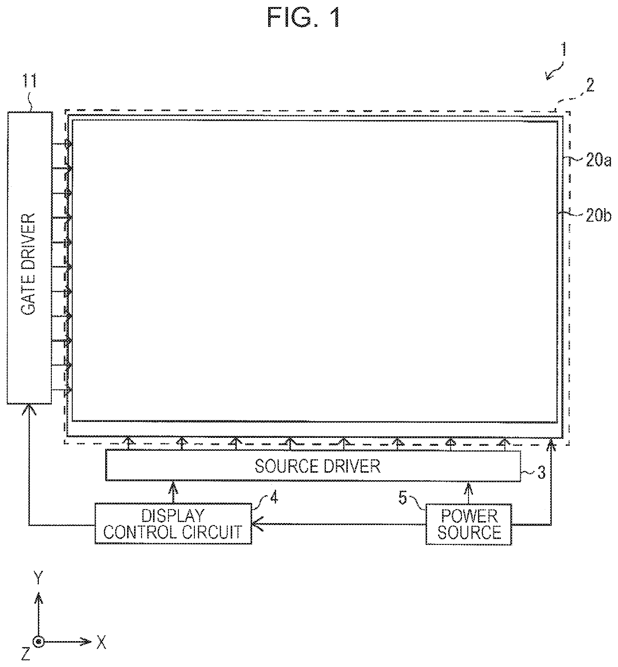
[0027]FIG. 1 is a top view depicting a schematic configuration of a liquid crystal display device 1 according to the present embodiment.

[0028]The liquid crystal display device 1 (display device) is provided with a display panel 2, a source driver 3, a gate driver 11 (gate driving circuit), a display control circuit 4, and a power source 5. The display panel 2 is provided with an active matrix substrate 20a, an opposite substrate 20b, and a liquid crystal layer (not depicted) held between the active matrix substrate 20a and the opposite substrate 20b. Although not depicted in FIG. 1, a polarizer is provided at the lower surface side (−Z side) of the active matrix substrate 20a and the upper surface side (+Z side) of the opposite substrate 20b. A black matrix, three color filters of red (R), green (G), and blue (...

embodiment 2

[0062]Another embodiment of the present disclosure is as follows when described on the basis of FIGS. 1, 5, 6, and 7. It should be noted that, for convenience of the description, members having the same functions as the members described in the aforementioned embodiment are denoted by the same reference signs and descriptions thereof are omitted.

(Configuration of Liquid Crystal Display Device and Active Matrix Substrate)

[0063]FIG. 1 is a top view depicting a schematic configuration of a liquid crystal display device according to the present embodiment.

[0064]A liquid crystal display device 1 is provided with a display panel 2, a source driver 3, a gate driver 11, a display control circuit 4, and a power source 5. The display panel 2 is provided with an active matrix substrate 20a, an opposite substrate 20b, and a liquid crystal layer (not depicted) held between these substrates.

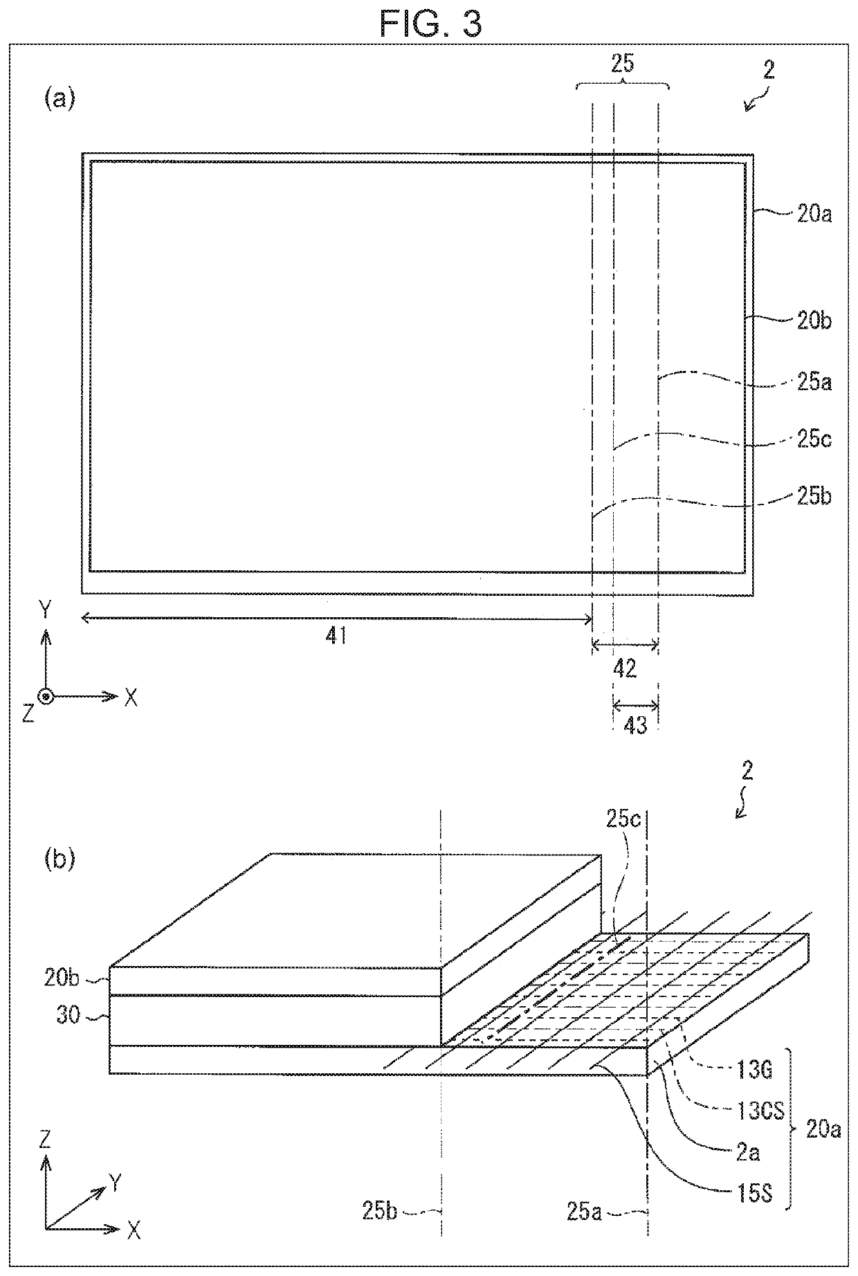
[0065]FIG. 5 is a top view depicting a schematic configuration of the active matrix substrate 20a.

[0066]Th...

embodiment 3

[0107]Another embodiment of the present disclosure is as follows when described on the basis of FIGS. 1, 2, and 8. It should be noted that, for convenience of the description, members having the same functions as the members described in the aforementioned embodiment are denoted by the same reference signs and descriptions thereof are omitted.

(Configuration of Liquid Crystal Display Device and Active Matrix Substrate)

[0108]FIG. 1 is a top view depicting a schematic configuration of a liquid crystal display device according to the present embodiment.

[0109]A liquid crystal display device 1 is provided with a display panel 2, a source driver 3, a gate driver 11, a display control circuit 4, and a power source 5. The display panel 2 is provided with an active matrix substrate 20a, an opposite substrate 20b, and a liquid crystal layer (not depicted) held between these substrates.

[0110]FIG. 2 is a top view depicting a schematic configuration of the active matrix substrate 20a.

[0111]The a...


PUM

PropertyMeasurementUnit
widthsaaaaaaaaaa
capacitanceaaaaaaaaaa
coloraaaaaaaaaa

Abstract

In the present disclosure, regions where a short circuit may have occurred due to dividing are isolated from a display region. In a gate line (13G) of an nth row, a gate line detour section (50G) that is provided corresponding to an intersection (CG,n,m) with a source line (15S) of an mth column has: a start section (51G) which is bent toward the −Y direction from a start position (XG,m(1), YG,n) that is in the −X direction relative to the intersection; and straddling sections (52G) which straddle a straight line (X=XS,m+dS / 2) that passes through a +X direction end of the intersection and extends in the Y axis direction.

Description

TECHNICAL FIELD[0001]The present disclosure relates to an active matrix substrate, a display panel, and a display device provided with the same, and particularly relates to altering the size of an active matrix substrate and a display panel including the same.BACKGROUND ART[0002]In display panels such as liquid crystal displays and electronic flat panel displays, there is a demand for altering the size of the display panel.[0003]However, when a display panel provided with an active matrix substrate is mechanically divided in order to alter the size, a short circuit may occur near the dividing line. This short circuit then causes a display defect in the display panel after the size alteration.[0004]In the invention described in PTL 1, in order to prevent a display defect caused by this short circuit, it is disclosed that short circuits are detected and repaired after a liquid crystal display has been divided.[0005]In the invention described in PTL 2, as a method for dividing wiring o...

Claims


Application Information

Patent Timeline
Patent Type & Authority Patents(United States)
IPC IPC(8): G02F1/1362G02F1/1368H01L27/12G02F1/1343G02F1/13G09F9/30
CPCG02F1/13H01L27/124G02F1/136286G02F1/1343G02F1/1368H01L27/1244G09F9/30G02F1/136259G02F1/133351G02F1/136263
Inventor OKAMOTO, SHOTANAKANISHI, YOUHEIKANEHIRO, MASAYUKI
Owner SHARP KK
Features
  • R&D
  • Intellectual Property
  • Life Sciences
  • Materials
  • Tech Scout
  • Unparalleled Data Quality
  • Higher Quality Content
  • 60% Fewer Hallucinations
Learn More