Supercharge Your Innovation With Domain-Expert AI Agents!

Capacitor and method of fabricating the same

a technology of capacitors and capacitors, applied in the field of capacitors, can solve the problems of unstable operation voltage of capacitors, inability to maintain capacitance at the same standard, and the size of semiconductor devices continues to become smaller, and achieve good reliability

Active Publication Date: 2020-03-24
UNITED MICROELECTRONICS CORP
View PDF4 Cites 0 Cited by
  • Summary
  • Abstract
  • Description
  • Claims
  • Application Information

AI Technical Summary

Benefits of technology

[0005]The invention provides a capacitor having good reliability and a method of fabricating the same.
[0026]Based on the above, in the capacitor and the method of fabricating the same provided in the embodiments of the invention, since the orthographic projection area of the second electrode on the dielectric layer is greater than the orthographic projection area of the first electrode on the dielectric layer, in the process of forming the second electrode on the dielectric, the dielectric is not damaged from the influence of the patterning process, and therefore the reliability of the capacitor is increased. Moreover, in the capacitor and the method of fabricating the same provided by the embodiments of the invention, the first via is further disposed on a portion of the second electrode not overlapped with the first electrode to prevent the dielectric from directly bearing the denser electric lines formed directly below the first via, such that the capacitor is not readily burned and the reliability of the capacitor is increased as a result.

Problems solved by technology

Among the various capacitors exemplified, other than the MIM capacitor, the capacitors all have at least one electrode formed by single-crystal silicon or polysilicon, and when bias voltage is applied to the single-crystal silicon or polysilicon electrode, a depletion region may be formed therein, such that the operating voltage of the capacitor is unstable and capacitance is not maintained at the same standard as a result.
However, as the size of semiconductor devices continues to become smaller, how to increase the reliability of the MIM capacitor to provide greater breakdown voltage (BVD) and longer time-dependent dielectric breakdown (TDDB) is an important issue researchers need to solve.

Method used


Image

  • Capacitor and method of fabricating the same
  • Capacitor and method of fabricating the same
  • Capacitor and method of fabricating the same

Examples


Embodiment Construction

[0031]The invention is more comprehensively described with reference to the figures of the present embodiments. However, the invention can also be implemented in various different forms, and is not limited to the embodiments in the present specification. The thicknesses of the layers and regions in the figures are enlarged for clarity. The same or similar reference numerals represent the same or similar devices and are not repeated in the following paragraphs.

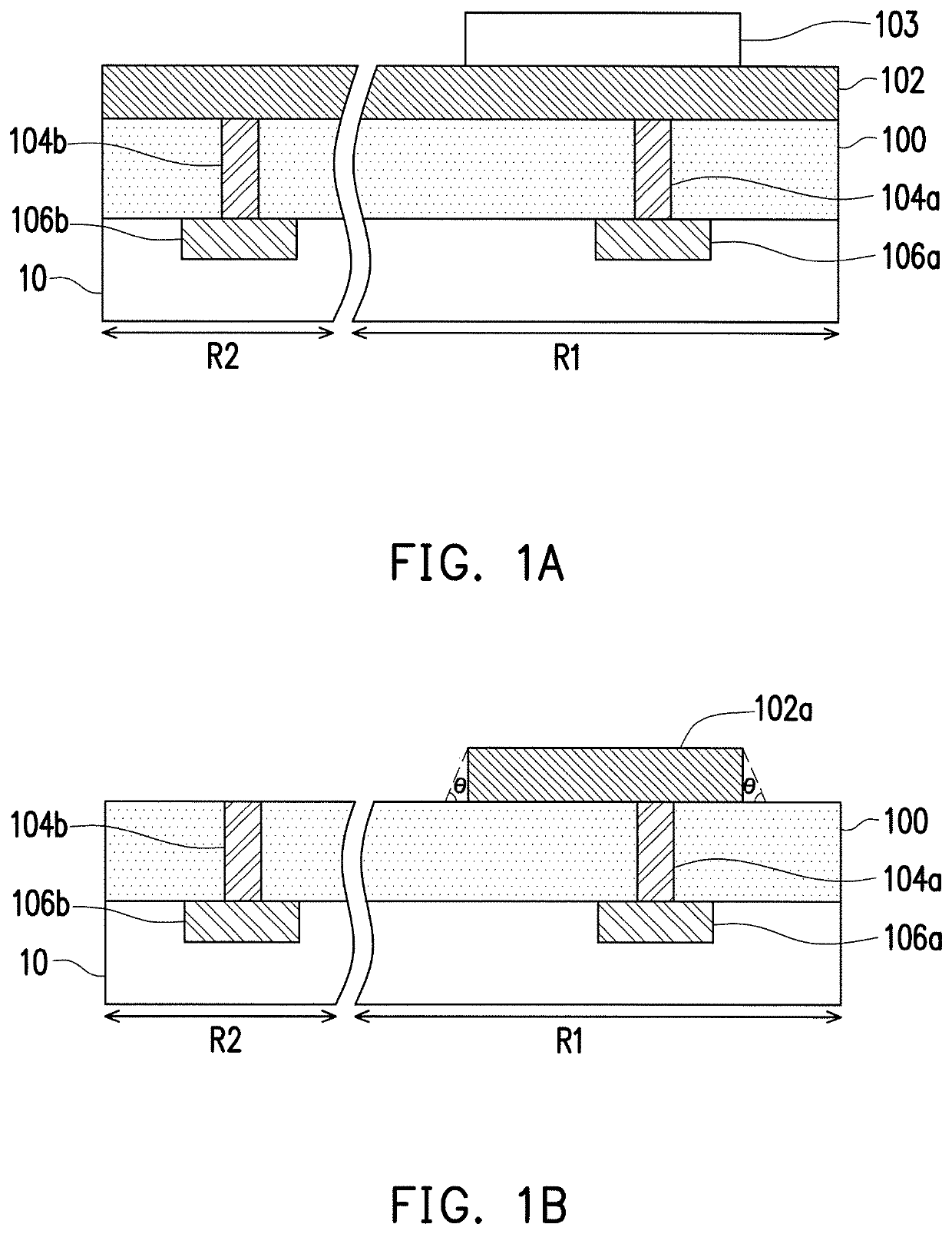
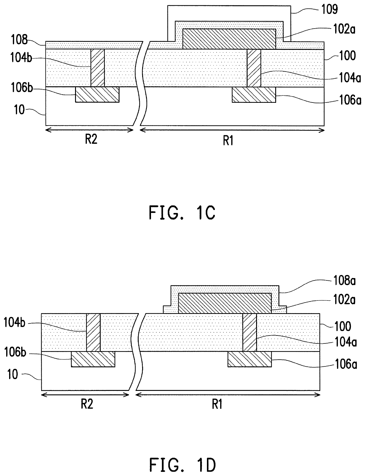
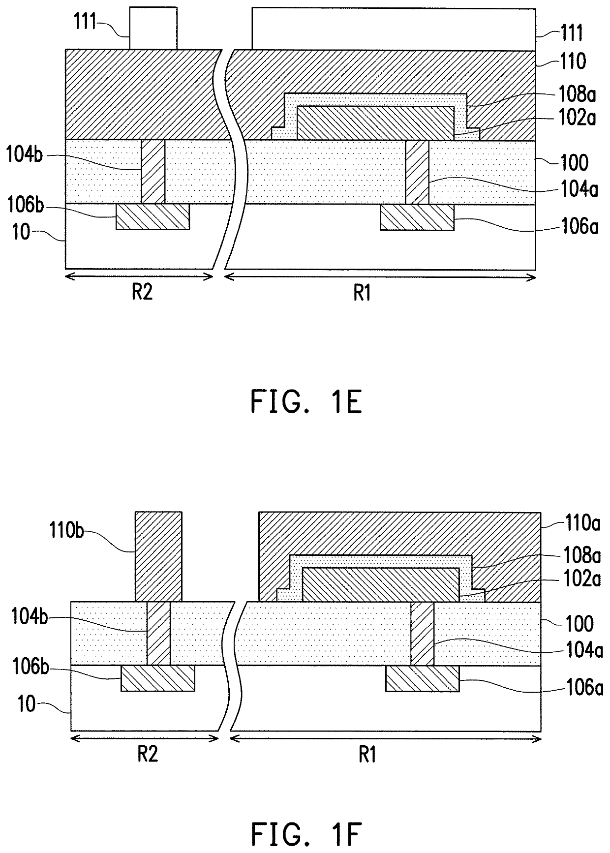
[0032]FIG. 1A to FIG. 1H are cross sections of a method of fabricating the capacitor according to an embodiment of the invention. FIG. 2 is a top view of a capacitor according to an embodiment of the invention and omits the dielectric layer and the second conductive layer located on the second electrode to clearly show the relative positions of the first electrode, the dielectric, the second electrode, and the first via.

[0033]Referring to FIG. 1A, a substrate 10 is provided. The substrate 10 includes a capacitance region R1 and...


PUM

PropertyMeasurementUnit
dielectric constantaaaaaaaaaa
angleaaaaaaaaaa
dielectric constantaaaaaaaaaa

Abstract

A capacitor includes a first electrode, a dielectric, and a second electrode. The first electrode is located on a dielectric layer. The dielectric covers the sidewall and the top surface of the first electrode. The second electrode covers the dielectric and the dielectric layer, wherein the orthographic projection area of the second electrode on the dielectric layer is greater than the orthographic projection area of the first electrode on the dielectric layer. The capacitor of the invention has good reliability.

Description

CROSS REFERENCE TO RELATED APPLICATION[0001]This application claims the priority benefits of China application serial no. 201710364072.8, filed on May 22, 2017. The entirety of the above-mentioned patent application is hereby incorporated by reference herein and made a part of specification.BACKGROUND OF THE INVENTIONField of the Invention[0002]The invention relates to a semiconductor structure and a method of fabricating the same, and more particularly, to a capacitor and a method of fabricating the same.Description of Related Art[0003]In integrated circuits, the capacitor includes a metal-oxide semiconductor (MOS) capacitor, a PN junction capacitor, a polysilicon-insulator-polysilicon (PIP) capacitor, and a metal-insulator-metal (MIM) capacitor. Among the various capacitors exemplified, other than the MIM capacitor, the capacitors all have at least one electrode formed by single-crystal silicon or polysilicon, and when bias voltage is applied to the single-crystal silicon or polys...

Claims


Application Information

Patent Timeline
Patent Type & Authority Patents(United States)
IPC IPC(8): H01G4/06H01G4/012H01L23/522H01G4/005H01G4/08H01G4/12H01L49/02H01G4/33
CPCH01L28/91H01G4/005H01G4/012H01G4/1272H01G4/33H01G4/06H01L23/5223H01G4/08H01L23/642H01L28/40H01L28/60
Inventor JEN, PO-HAN
Owner UNITED MICROELECTRONICS CORP
Features
  • R&D
  • Intellectual Property
  • Life Sciences
  • Materials
  • Tech Scout
  • Unparalleled Data Quality
  • Higher Quality Content
  • 60% Fewer Hallucinations
Learn More