Substrate for semiconductor devices
a technology for semiconductor devices and substrates, applied in semiconductor devices, semiconductor/solid-state device details, electrical apparatus, etc., can solve the problems of reduced insulation properties, and solder overflow from insulating substrates
- Summary
- Abstract
- Description
- Claims
- Application Information
AI Technical Summary
Benefits of technology
Problems solved by technology
Method used
Image

Examples
example 1
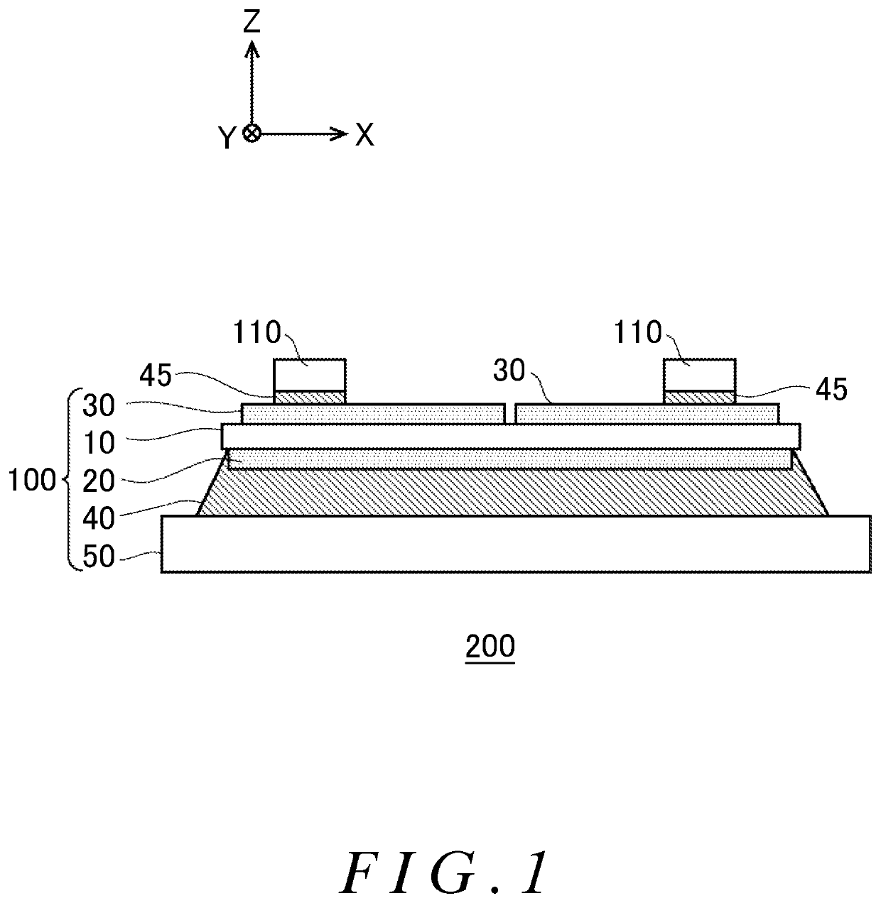
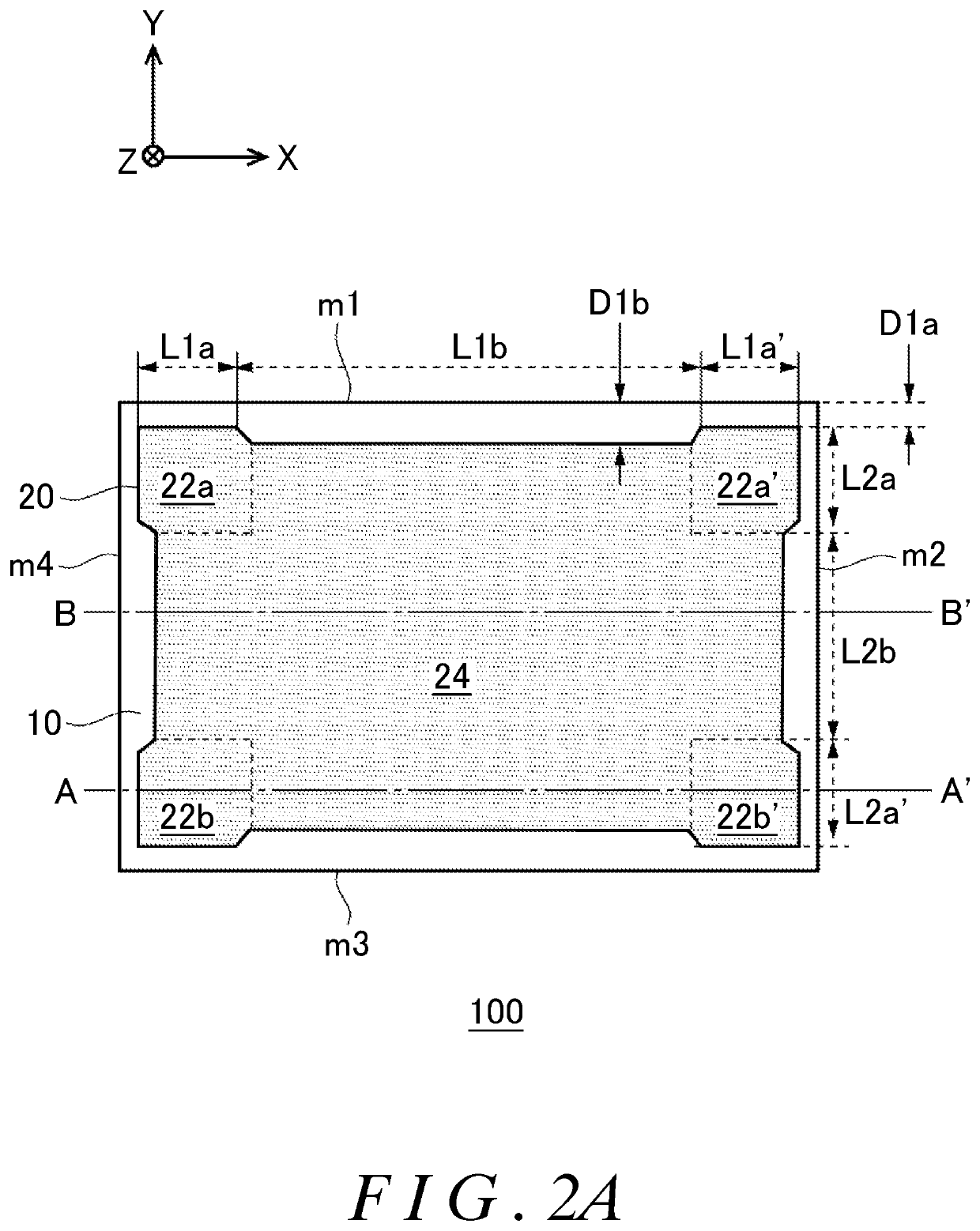
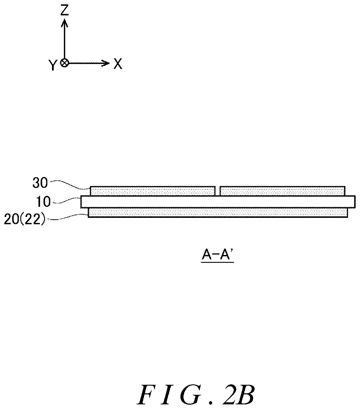
[0047]FIG. 2A illustrates an exemplary plan view of an insulative substrate in accordance with Example 1. FIG. 2B illustrates an exemplary cross-sectional view taken along A-A′ of the insulative substrate in accordance with Example 1. FIG. 2C illustrates an exemplary cross-sectional view taken along B-B′ of a substrate 100 for semiconductor devices in accordance with Example 1. Note that FIG. 2A is viewed from a negative side of the Z axis to illustrate the shape of the first metal board 20.
[0048]The insulating substrate 10 has a rectangular shape in a planar view. The insulating substrate 10 of the present example includes a first side m1, a second side m2, a third side m3 and a fourth side m4. The first side m1 and the third side m3 correspond to longer sides. The second side m2 and the fourth side m4 correspond to shorter sides of the rectangular shape.
[0049]The first metal board 20 has a polygon shape in a planar view. Although the first metal board 20 of the present example has...
example 2
[0066]FIG. 6 illustrates an exemplary configuration of a substrate 100 for semiconductor devices in accordance with Example 2. For the substrate 100 for semiconductor devices of the present example, insulating substrates 10a, 10b, first metal boards 20a, 20b and a heat releasing board 50 are shown. Other configurations are omitted for the sake of simplicity of the description.
[0067]The insulating substrate 10a has an approximately square shape in a planar view. The insulating substrate 10b has an approximately rectangular shape in a planar view. In one example, the insulating substrate 10a and the insulating substrate 10b include a semiconductor chip 110 formed thereon, respectively.
[0068]The heat releasing board 50 has a rectangular shape in a planar view. The heat releasing board 50 is sized to allow at least the insulating substrate 10a and the insulating substrate 10b to be placed thereon. The heat releasing board 50 of the present example includes soldered portions 60, 65.
[0069...
example 3
[0083]FIG. 8 illustrates an exemplary configuration of a substrate 100 for semiconductor devices in accordance with Example 3. The substrate 100 for semiconductor devices of the present example comprises a first metal board 20b of a shape different from that of the substrate 100 for semiconductor devices in accordance with Example 2.
[0084]The first metal board 20a is provided to correspond to the insulating substrate 10a. The first metal board 20a has an approximately square shape if the insulating substrate 10a has a square shape. The first metal board 20a of the present example includes a corner portion 22 and a center portion 24 on each side.
[0085]The first metal board 20b is provided to correspond to the insulating substrate 10b. The first metal board 20b has an approximately rectangular shape if the insulating substrate 10b has a rectangular shape. The first metal board 20b of the present example includes a side having the corner portion 22 and the center portion 24 formed ther...
PUM
| Property | Measurement | Unit |
|---|---|---|
| thickness | aaaaa | aaaaa |
| thickness | aaaaa | aaaaa |
| creepage distance | aaaaa | aaaaa |
Abstract
Description
Claims
Application Information
PatSnap Eureka turns technology decisions into work you can execute. Powered by our Innovation Knowledge Graph, it runs expert workflows across engineering, life sciences, materials and intellectual property. Get your review-ready output in minutes.


