Image stitching method and electronic device using the same

a technology of image stitching and electronic devices, applied in the field of image stitching methods and electronic devices, can solve the problems of large amount of time and resources, image stitching speed normally cannot meet the low-delay requirement for real-time viewing, and the use of foldable multi-lens products, so as to achieve the effect of reducing the time for locating an overlapped region of images using an image stitching algorithm and increasing the image stitching speed

Active Publication Date: 2020-06-16
ACER INC
View PDF6 Cites 0 Cited by
  • Summary
  • Abstract
  • Description
  • Claims
  • Application Information

AI Technical Summary

Benefits of technology

[0006]The present disclosure relates to an image stitching method and an electronic device using the same. A physical bending information of the base is detected by the sensing module mounted on the base, and the current bending angle of the base is estimated according to the obtained physical bending information to locate corresponding overlapping information. Therefore, the time for locating an overlapping region of images by using an image stitching algorithm can be effectively reduced, and the image stitching speed can be increased.

Problems solved by technology

However, the off-line image stitching algorithms are subjected to certain restrictions regarding the use of foldable multi-lens products.
The difficulties currently encountered by the real-time stitching algorithms are that: during the stitching process, the feature points of each image need to be completely scanned to locate the overlapping region of images.
However, since it takes a large amount of time and resources to scan the complete image, the image stitching speed normally cannot meet the low-delay requirement for real-time viewing.

Method used


Image

  • Image stitching method and electronic device using the same
  • Image stitching method and electronic device using the same
  • Image stitching method and electronic device using the same

Examples


Embodiment Construction

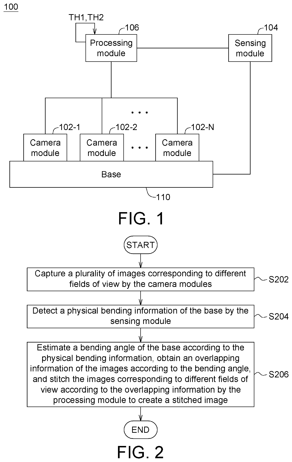
[0014]FIG. 1 is a block diagram of an electronic device 100 according to an embodiment of the present disclosure.

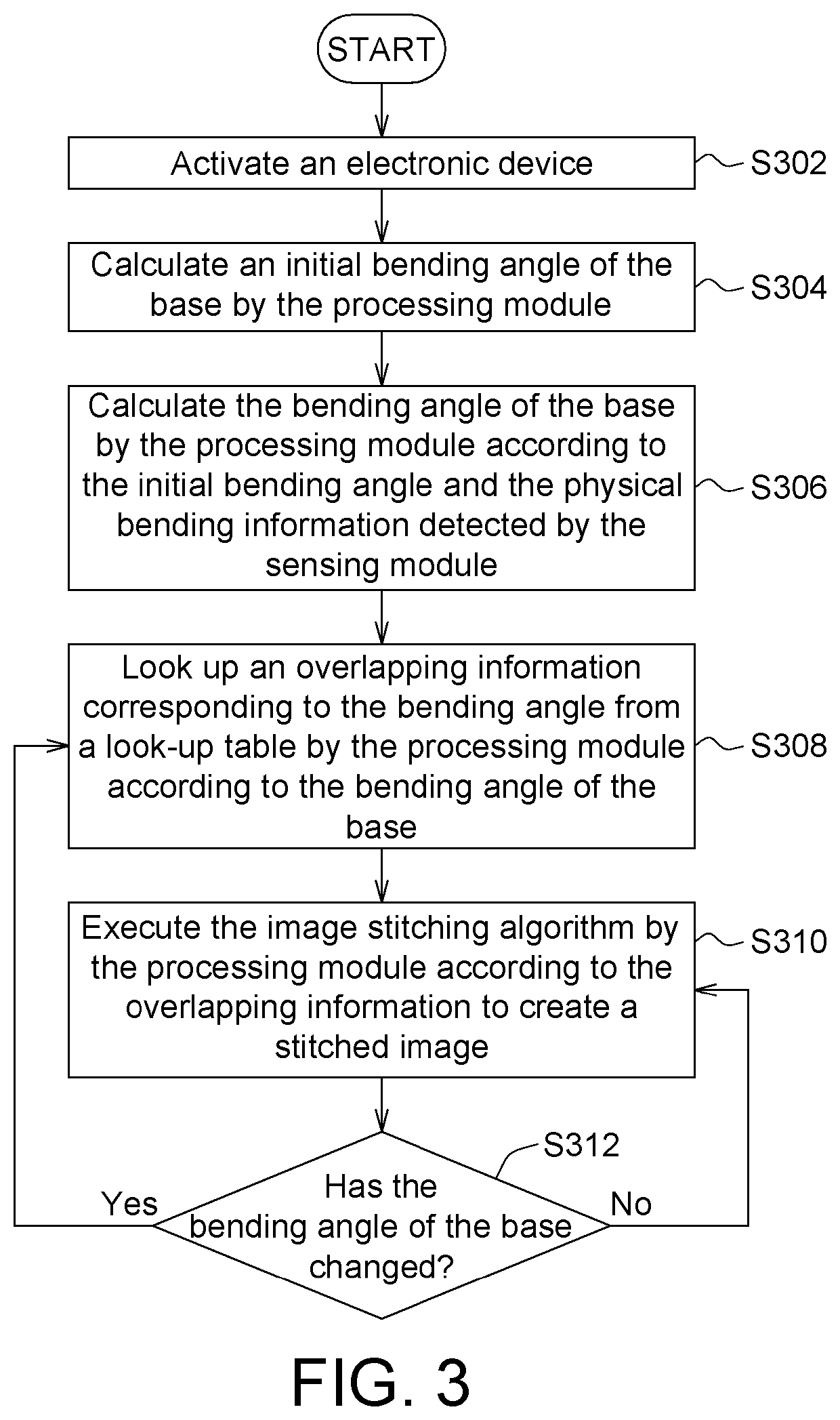
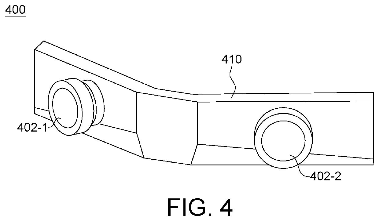
[0015]Referring to FIG. 1, the electronic device 100 includes a bendable base 110, a plurality of camera modules 102-1 to 102-N (N is a positive integer larger than 1), a sensing module 104 and a processing module 106. The base 110 can have a bendable mechanism (such as a pivot) formed of any bendable material such as plastics or resin. The camera modules 102-1 to 102-N can be realized by charge-coupled device (CCD) sensors, complementary metal-oxide-semiconductor (CMOS) sensors or other camera devices. The sensing module 104 can be realized by an accelerometer, a gyroscope, a distance sensor, a resistance / capacitance sensing component or any sensor capable of sensing the change in the bending angle of the base 110. The processing module 106 can be realize by a central processing unit (CPU), a microprocessor, digital signal processor (DSP), a programmable controller, an a...


PUM


Abstract

An electronic device including a bendable base, a plurality of camera modules, a sensing module and a processing module is provided. The camera modules are mounted on the base, and may capture a plurality of images corresponding to different fields of view. The sensing module is coupled to the base for detecting a physical bending information of the base. The processing module is coupled to the camera module and the sensing module for estimating a bending angle of the base according to the physical bending information, obtaining an overlapping information of the images according to the bending angle, and stitching the images according to the overlapping information to create a stitched image.

Description

[0001]This application claims the benefit of Taiwan application Serial No. 107108230, filed Mar. 12, 2018, the subject matter of which is incorporated herein by reference.BACKGROUND OF THE INVENTIONField of the Invention[0002]The invention relates in general to an image stitching method and an electronic device using the same.Description of the Related Art[0003]Along with the advance in the micro-camera technology, more and more products can concurrently use multiple cameras to generate images with a wider field of view, and can be used in capturing panorama images, the monitoring system, and the around view monitoring (AVM) system. Generally speaking, such products can widen the field of view of the outputted images by combining the images captured using multiple lenses, and the widening process is completed by using an image stitching algorithm.[0004]The image stitching algorithm is used for cropping, collaging and stitching a plurality of images corresponding to different fields ...

Claims


Application Information

Patent Timeline
Patent Type & Authority Patents(United States)
IPC IPC(8): G06T3/40G06T7/70H04N5/232H04N5/247G06K9/62
CPCH04N5/247G06T7/70G06T3/4038G06K9/6202H04N5/23238G06T2207/30244H04N23/50H04N23/45H04N23/698H04N23/90
Inventor CHENG, CHEN-JUCLARES, SERGIO CANTERO
Owner ACER INC
Why Eureka
Try Eureka